0 Preface
The sinusoidal signal source plays an important role in the laboratory and electronic engineering design. The traditional sinusoidal signal source is generally expensive according to actual needs, the performance at low frequency output is not good and it is not convenient to automatically adjust, and the engineering practicability is poor. The design of this paper makes a sinusoidal signal generator at a lower cost, and can be used as an excitation sinusoidal signal for inducing a magnetic field measuring instrument in nuclear magnetic resonance, or as a teaching demonstration signal source for modulation.
The sinusoidal signal generator is mainly composed of two parts: a sine wave signal generator and generating amplitude modulation, frequency modulation, and keying signals. The sinusoidal signal generator uses direct digital frequency synthesis DDS technology to implement sinusoidal signal lookup table and address scanning on the CPLD, and a sinusoidal signal can be obtained through the D/A output. It has high frequency stability and wide frequency range, and it is easy to achieve frequency stepping of 100 Hz. The all-digital structure is easy to integrate, the output phase is continuous, and the frequency, phase and amplitude can be programmed.
The modulation, frequency modulation and keying signals can be generated by frequency modulation and amplitude modulation chips. However, the frequency modulation and amplitude modulation function achieved by this method is better for a specific frequency and specific modulation degree and frequency offset. It is difficult to achieve the case where the variable and modulation degrees and frequency offsets are arbitrarily set. In this paper, CPLD and single-chip AT89S52 can not only realize sine wave signal with adjustable frequency range, but also can realize FM FM easily by adding corresponding digital control algorithm inside CPLD. AM AM and keyed PSK, ASK digital modulation function is beneficial. Improve the overall performance and reliability of the system. The sinusoidal signal generation part can be implemented in a CPLD (EP1K30), which greatly simplifies the hardware circuit, facilitates function expansion, and creates conditions for further system integration.
1 Theoretical analysis and calculation
1.1 Generation of sinusoidal waveforms
The one-way DDS consists of a numerically controlled oscillation source (NCO) composed of an Nbit phase accumulator and a ROM read-only memory (sinusoidal look-up table), a digital-to-analog converter (DAC), and a low-pass smoothing filter (LPF). The basic structure of DDS.
In Figure 1, fc is the clock frequency, K is the frequency control word, N is the word length of the phase accumulator, M is the number of ROM address lines, L is the ROM data line width, and fo is the output frequency. The phase accumulator consists of a cascade of full adders and accumulator registers. Under the control of the clock frequency fc, the input frequency control word K is accumulated, and an overflow occurs when the full amount is accumulated. The output of the phase accumulator corresponds to the phase of the synthesized periodic signal at that time, and this phase is periodic, varying in the range of 0 to 2Ï€. The number of phase accumulators is N, and the maximum output is 2N-1, corresponding to the phase of 2Ï€. When accumulating 1 time, a corresponding phase code is output, and the address is obtained by looking up the table to obtain the signal amplitude value of the corresponding phase. By converting, a signal output waveform of a certain frequency can be obtained, and the low-pass filter smoothes the output signal waveform to filter out clutter and harmonics. Since the control word K is accumulated by 2N/K times, the phase accumulator overflows and completes one cycle operation, so the output frequency fo is determined by fc and K together, that is, fo=fcK/2N and K "2N-1, DDS is obtained. The minimum resolution is up to fc/2N. Theoretically, by setting the value of the number of bits N of the DDS phase accumulator, the frequency control word K, and the clock frequency fc, an output of any frequency can be generated. According to the frequency stepping requirement of 100 Hz, the number of bits of the accumulator is 19 bits, and the clock frequency fc should be calculated to be 52.4288 MHz. The cumulative error of the step is corrected by the software compensation method, and the existing stepping of 100 Hz is completely accurately realized by using the existing 52.416 0 MHz crystal oscillator.
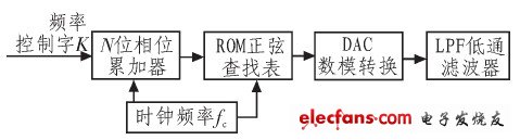
Figure 1 Schematic diagram of a DDS-based sinusoidal signal generator
1.2 Generate analog amplitude modulated signal
The modulation signal is used to control the amplitude of the high-frequency oscillation so that the amount of change in amplitude varies in proportion to the modulation signal. This process is called amplitude modulation. If the carrier is uc=Uc cosωct and the modulation signal is f(t)=cosΩt, then the amplitude modulation wave is
![]()
The ordinary amplitude modulation wave is realized by the analog multiplier, but the peripheral circuit is complicated, and changing the modulation degree needs to change the parameters of the circuit component, which is complicated to implement. The digital amplitude modulation can be flexibly implemented by using the CPLD chip combined with the DDS technology. The principle is shown in FIG. 2 .
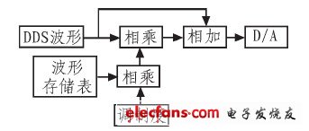
Figure 2 amplitude modulation schematic
The waveform signal generated by the DDS is used as a carrier. The sinusoidal waveform storage table with a modulation signal of 1 kHz is generated in the microcontroller, and the modulation degree ma (10% to 100%) set by the keyboard is multiplied by the data in the storage table. The CPLD is multiplied by the waveform obtained by the DDS, and then added to the DDS signal to generate the corresponding digital amplitude modulation wave code, and the analog amplitude modulation signal is obtained by D/A conversion.
1.3 Generate analog frequency modulated signals
In continuous wave modulation, the carrier can be expressed as uc=Uc cosωct, and the modulation signal is UΩ(t). The frequency of the FM wave is proportional to the modulation signal, so the instantaneous angular frequency of the FM wave is in addition to the carrier angular frequency ωc. Also, a portion proportional to the modulation signal is added, where kf is a proportional coefficient, which is a frequency change caused by the intensity of the unit modulated signal. The maximum value Δωf of Δωf(t) is called the maximum frequency offset, which is reflected in the frequency as f(t)=fc+△fcos(2πft), and the expression of the FM wave:
![]()
Figure 3 shows the CPLD digital frequency modulation circuit. When the frequency offset is 5 K, the control word is 50. The cosine waveform is multiplied by 50 and added to the frequency control word transmitted by the MCU. The DDS module can be sent to the DDS module for D/A conversion. The output frequency modulation wave is shown in Figure 4.
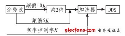
Figure 3 CPLD digital frequency modulation circuit diagram
Figure 4 Frequency modulation design schematic
Brushed Dc Motor,Dc Brushed Motor,Brushed Rc Motors,High Torque Brushed Dc Motor
Changzhou Sherry International Trading Co., Ltd. , https://www.sherry-motor.com