DR2 (Double Data Rate 2, double data rate, version 2) SDRAM is an DDR SDRAM-based upgrade storage technology developed by the JEDEC standards organization. Compared with DDR SDRAM, although it still maintains the characteristics of two data transmissions in one clock cycle, DDR2 SDRAM has significantly improved in data transmission rate, delay, power consumption, etc., and these performance improvements, the main source Improvements in the following technologies: ODT, Post CAS, 4n data prefetching, packaging, etc.
* ODT
ODT (On-Die Termination), which is the internal termination of the chip.
In DDR SDRAM applications, a large number of external resistors need to be pulled up to the VTT level (1.25V) for signal matching. Taking a 16-bit chip as an example, the following signals need to be matched in this way: CK, CK#, DQ [15:0], LDQS, UDQS, ADDR[10:0], RAS#, CAS#, WE#, that is, a chip requires 34 external pull-up resistors, which greatly takes up valuable PCB area. At the same time, since DQ[15:0], LDQS, UDQS and other signals are bidirectional signals, that is, when reading and writing, there are different requirements for the position of the matching resistor, so it is difficult to achieve the best in both directions in the resistance layout. Signal integrity.
In DDR2 SDRAM, many external matching resistors are moved to the inside of the chip using ODT technology, which saves a lot of PCB board area. In addition, the ODT technology allows the memory controller (such as the MPC8548 CPU below) to control the value of the matching resistor and its switching state by configuring the internal registers of the DDR2 SDRAM and controlling the ODT signal, thereby enabling the most read and write operations. Good signal integrity.
This article refers to the address: http://
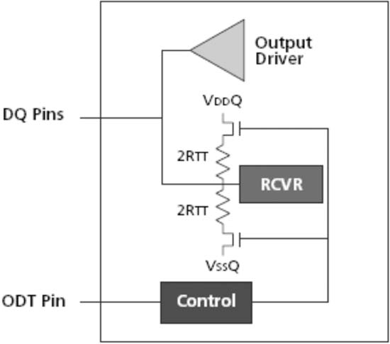
Figure 1 ODT function chart
The DDR2 SDRAM chip provides an ODT pin to control the termination resistor inside the chip. In the case of a load with only one DDR2 SDRAM chip as the memory controller, when the DDR2 SDRAM is used as the receiving end, the ODT pin is high to turn on the internal termination resistor of the chip; during the read operation, due to the DDR2 SDRAM Transmitter, so the ODT pin is low to turn off the chip's internal termination resistor. The state of the ODT pin is controlled by a memory controller such as the MPC8548.
The ODT termination resistor value RTT can be set by the EMR register inside the DDR2 SDRAM: first configure EMR[15:14]=01 to select this register to work in EMR (Extended Mode Register) mode, then pass EMR[6] and EMR [2] Two bits to set the value of the internal RTT, allowing the selection of four modes of RTT off, 75 ohms, 150 ohms, and 50 ohms. Taking the 75 ohm mode as an example, in Figure 1, the pull-up and pull-down resistors inside the DQ pin will be configured to be 150 ohms.
It should be noted that the ODT technology of DDR2 SDRAM only implements internal matching for signals such as DQ, DQS, and DM (including DQS# signals when differential DQS is selected). Addresses and control signals, etc. still need to be matched externally.
* Posted CAS
Take DDR2 SDRAM as an example.
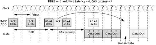
Figure 2 gap problem when reading multiple blocks of data
Like DDR SDRAM, DDR2 SDRAM is addressed by a combination of Bank (Block Address), Row (Row Address) and Column (Column Address). Each operation of the DDR2 SDRAM starts with the ACTIVE command (the ACT command of Figure 2, implemented by the active #RAS signal). At the same time as the command is issued, the Bank and Row addresses of this operation are issued through the address signal line. After waiting for the tRCD time, the READ/AUTO PRECHARGE command (the RD AP command of Figure 2 is implemented by the active #CAS signal) is issued. The function of the command is to issue a read command and simultaneously issue the Column address of the operation through the address signal line. Finally, after waiting for the CAS Latency time, the data is output via the data bus.
As the storage space of DDR2 SDRAM has increased relative to DDR SDRAM, the number of banks has also increased. For example, the maximum capacity of a DDR SDRAM chip is 1 Gbit, the number of banks is 4, and the maximum capacity of a DDR2 SDRAM chip is 2 Gbit, and the number of banks reaches 8. The number of banks for DDR SDRAM is at least 2, while the number of banks for DDR2 SDRAM is at least 4. In order to improve performance, it is often necessary to insert an operation on the next Bank before the completion of a Bank operation. As shown in Figure 2, after issuing the ACT command to Bank0, there is no need to wait for the corresponding RD AP command to be issued. Only the TTL command for another bank can be issued by satisfying the tRRD time requirement.
The N-NET Ethernet over coax (EOC) allows IP cameras to transmit over Coax cabling. The Ethernet over coax technology allows the system to extend IP cameras beyond cable distance limitations and also acts as a PoE inserter.
N-net Ethernet And Power Over UTP Cable Converter is an Ethernet extender over UTP cable. It can transmit over telephone line, Ethernet cable, and twisted pair. It is provided with excellent lightning protection and anti-interference capacity.
N-net Ethernet And Power Over Coax Converter is a conversion device for Ethernet over Coax. It can be used in pair or one to multi.The equipment can transmit by telephone line, Ethernet cable, UTP or coax, etc all kinds of common cables.
Ethernet Over Coax Converter,Coax To Ethernet,Ethernet Over Coax Adapter,Coax To Ethernet Adapter
Shenzhen N-net High-Tech Co.,Ltd , http://www.nnetswitch.com