In this paper, DDR SDRAM is used as the storage unit. By using the clock double edge transmission data without changing the system clock, the transmission bandwidth of the same frequency chip is doubled on the basis of SDRAM, which satisfies the needs of high bandwidth buffer. .
1 DDR memory introduction
DDR memory is a dual data rate synchronous dynamic random access memory. Like the early single data rate synchronous dynamic random access memory, the internal memory unit uses capacitor charging to save data. Therefore, it is necessary to constantly charge the capacitor to maintain data. This is called "Refresh". The SDRAM data bus accesses data on the rising edge of each clock, while the DDR SDRAM accesses data on both the rising and falling edges of each clock, so that the data bus bandwidth is constant with the same data bus width and clock frequency. Doubled the gain.
2 system design
Designed using Xilinx's Sptan3a-dsp 1800a as the main controller, Micron's MT64V32X16 chip is used as the storage medium, and the maximum storage capacity is 512M. The logic part of the system consists of arbitration module, input buffer module, scheduling decision module, address conversion module and DDR interface control module. The block diagram is shown in Figure 1.
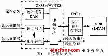
The arbitration module in the core controller generates the corresponding control commands. After the power-on initialization reset, and during the system running, the refresh command, the write operation command and the read operation command are issued for the work priority; the DDR interface control module implements the core controller command according to the basic timing of the DDR chip operation. For the information transmission of the physical chip; the south DDR chip has non-real-time operation characteristics, the internal input buffer RAM must be used for basic real-time data buffering; and the address conversion module and the scheduling decision module cooperate with the internal input buffer RAM to complete the DDR chip. Mapping work for internal storage space.
3 DDR core controller design
DDR memory is a kind of high-speed memory chip with relatively complicated instructions. It must be initialized after power-on to perform other operations. It does not support single-cycle read and write operations, and only supports burst read and write operations of 2, 4, and 8 cycles. In addition, due to its capacitive characteristics, the DDR chip is unstable in data storage, and needs to be refreshed in a certain period of time to ensure that data is not lost. Therefore, there are dozens of instructions in the DDR operation. However, in this design, the DDR interface controller uses the DDR IP provided by Xilinx, so that the arbitration module in the core controller only needs to use four instructions of idle, initialization, read operation and write operation to complete the DDR-SDRAM. Operation greatly reduces the design difficulty. Since the design is aimed at eliminating the jitter of IP data from the network, and finally distributing the IP data to 512 channels, which greatly exceeds the requirements of the previous design for DDR, this paper proposes the design shown in Figure 1 here. DDR memory for high speed, large capacity and multi-channel design applications:
(1) Input Cache Module
The input buffer consists of a RAM plus external logic that buffers the TS packet payload that has been input but has not yet been written to the DDR. After the arbitration module issues a signal that allows writing, the data packet in the input buffer is passed to the arbitration module, and the corresponding storage space is released. According to the working mode of DDR and DVB-C characteristics, the data transmission of the input buffer is realized in units of TS packets, and 192 bytes of continuous burst transmission are realized.
(2) Scheduling decision module
The scheduling decision module receives the read request queue information, and realizes the decision of scheduling the queue out of the FIFO with the largest amount of data in the same bank when reading the data. This module saves the current number of packets in each channel FIFO.
(3) Address translation module
The address translation module is responsible for mapping the channel number and the internal memory space of the DDR SDRAM chip. The variables stored in this module include the block start address, block end address, FIFO header offset, and FIFO tail offset of each channel in DDR SDRAM.
(4) Arbitration module
The arbitration module generates corresponding control commands, and issues idle instructions, initialization instructions, write operation instructions, and read operation instructions for the work priority.
Air Filter: Prevents harmful debris, dirt and contaminants from entering your engine.
Engine protection is the name of the game.So is engine performance. Acceleration can improve up to after an old, dirty air filter is replaced. Our Pennzoil air filters are engineered to trap harmful contaminants that can damage your engine.
Old and dirty air filters lead to reduced engine power, decreased throttle response, weaker acceleration and increased engine wear. Sounds ugly. Well, it is, and you should have it replaced when it gets bad.
Air Filter
Automotive Air Filter,Car Air Filter,Air Filter Cartridge
Donguan Bronco Filter Co., Ltd , https://www.broncofilter-cn.com