0 Preface
In recent years, with the rapid development of wireless communication services, communication frequency bands have become increasingly crowded. In 1985, the United States Federal Communications Commission (FCC) authorized ordinary users to use 902MHz, 2.4GHz and 5.8GHz three "industrial, scientific, medical" (ISM) frequency bands. The ISM frequency band provides product bands that can be directly used without applying for low transmission power for wireless communication equipment, which greatly promotes the development of the wireless communication industry. Although the current wireless digital communication technology is quite mature, radio frequency design is still the bottleneck of mobile communication design. The design of the radio frequency circuit mainly revolves around the requirements of low cost, low power consumption, high integration, high operating frequency and light weight. The research of the radio frequency circuit in the ISM band is of great significance to the future development of wireless communication. Many literatures at home and abroad have done research on this. Document [2] introduced the design of the 2.4GHz transmitter under the environment of wireless high-speed data communication. Literature [3] introduced a low-power CMOS integrated transmitter design.
ADS (AdvancedDesignSystem) software is a large-scale comprehensive design software developed by Agilent on the basis of HPEESOF series EDA software. It is powerful and can provide simulation and optimized design of various radio frequency microwave circuits and is widely used in the fields of communications and aerospace. This article mainly introduces how to use ADS to design the RF front-end of the transceiver system, and carry out some simulations under the analog and digital design environment of ADS.
l Modeling and simulation of the transmitter
Because the design is based on the existing intermediate frequency modulation and demodulation hardware in the laboratory, the transmitter and receiver do not consider the signal modulation and demodulation process. The intermediate frequency modulation module in the laboratory can output a 40MHz modulated intermediate frequency signal of about 8 to 10dBm. After analysis and selection, each module at the transmitter end is designed with reference to the parameters of the integrated module of MAXlM. The local oscillator uses the MAX2700. The MAX2700 is a voltage-controlled oscillator, and it can output a 2.4GHz signal by designing a suitable peripheral circuit. The mixer uses the MAX2660. The MAX2660 is an active mixer that can provide a certain gain. The power amplifier uses MAX2240, the maximum output power of MAX2240 is 15.3dBm. The filter used at the transmitter can be designed using the filter design tool in the ADS software. Since the insertion loss of the actual filter is about 1 to 2dB, the insertion loss of the filter in this design is 1dB. Modeling is done through the analog circuit design environment in ADS software.
In the transmitter model, the intermediate frequency signal is 40MHz, -10dBm signal. In the simulation design environment of ADS, the transmitter is designed and budgeted. The simulation is mainly to measure the gain, noise figure, and third-order intermodulation intercept point of each module. The simulation process is shown in Figure 1.
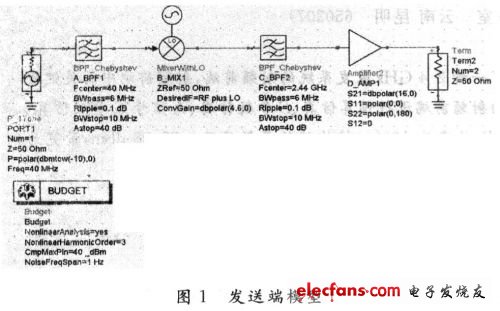
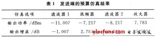
As can be seen from the simulation results in Table 1, the total gain of the entire transmitter is 17.783dB. The input intermediate frequency signal is -10dBm, so the RF signal output by the power amplifier is 7.783dBm.
2 Modeling and simulation of the receiving end
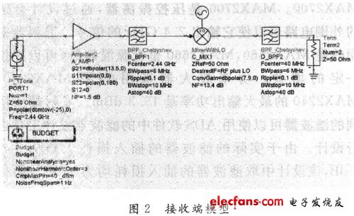
The receiver must consider gain, noise figure, sensitivity and other factors in the design, which is more complicated than the design of the transmitter. Because the receiving end contains many active devices, the nonlinearity of the active devices will have a great impact on the entire receiving system, such as gain compression when only one signal is input, and mutual modulation when more than two signals are input. Wait. In this design, the intermediate frequency demodulation module also requires a signal size of 8 ~ 10dBm. After analysis, the low-noise amplifier uses MAX2641, the gain of MAX2641 is 13.5dB, and the noise figure is 1.5dB. The mixer uses MAX2682, the gain of MAX2682 is 7.9dB, the noise figure is 13.4dB, the local oscillator is the same as the transmitter. Use ADS to model the receiving end, as shown in Figure 2.
Since the parameters of each module are known, the total noise figure of the system and the third-order intermodulation intercept point can be obtained through calculation.
The noise figure is defined as the ratio of the system input signal-to-noise power ratio (SNR) i = Pi / N, and the output signal-to-noise power ratio (SNR) o = Po / No, which is commonly expressed by F. The noise figure characterizes the degree of deterioration of the signal-to-noise ratio caused by the internal noise of the system after the signal passes through the system. The noise figure is often expressed in NF (in dB). According to the cascade of noise figure:
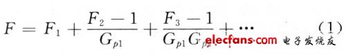
The total noise figure of the system can be calculated. The total noise figure of the system is viewed from the low-noise amplifier in Figure 3 toward the output. The noise figure exhibited can also be understood as when the received signal is transmitted by the low-noise amplifier to The degree of deterioration of the signal-to-noise ratio at the output and receiver. Using formula (1), the noise figure of the system is F = 2.582dB and NF = 4.12dB.
The third-order intercept point IP3 is defined as the point where the third-order intermodulation power reaches equal to the fundamental power, the input power corresponding to this point is expressed as IIP3, and the output power corresponding to this point is expressed as OIP3. According to the cascade of the third-order intermodulation intercept point:
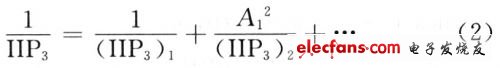
It is available that the total IIP3 of the system = -9.75 dBm. Also in the simulation design environment, budget simulation is performed on the receiving end, and the simulation results are shown in Table 2.
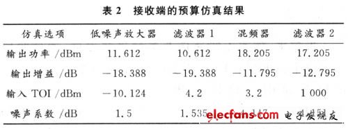
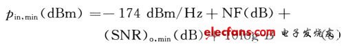
From the simulation results in Table 2, it can be seen that the gain of the entire receiving end is 17.205dB. Assuming that the signal received by the receiving antenna is -30dBm, the received intermediate frequency signal size is -12.795dBm. The simulation value of the intermediate frequency signal is slightly lower than the signal size required by the intermediate frequency receiving end, which can be increased by driving the amplifier. In addition, it can be seen from the simulation results that the total noise figure at the receiving end is 4.151dB, while the calculated result is 4.12dB. The third-order input intercept point of the receiving end of the simulation is -10.124 dBm, and the calculated value is -9.75 dBm. There is a certain difference in the above results, which is caused by factors such as gain compression. A very important indicator of the receiver is the sensitivity, which is defined as: the minimum input signal level that the receiver can detect under the given signal-to-noise ratio. The sensitivity is related to the required output signal quality, that is, the output signal-to-noise ratio, and also to the noise level of the receiver itself. The sensitivity of the receiver can be calculated by the following formula:

Assuming that the input of the receiver meets the conjugate matching, the noise power generated by the source internal resistance Rs delivered to the receiver is its rated output, namely
Rated output
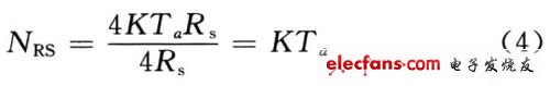
Assuming Ta = 290K, then NRS = -174dBm / Hz. So the sensitivity can be expressed as:
The electrolyte material inside the Electrolytic capacitor, which has charge storage, is divided into positive and negative polarity, similar to the battery, and cannot be connected backwards.A metal substrate having an oxide film attached to a positive electrode and a negative electrode connected to an electrolyte (solid and non-solid) through a metal plate.
Nonpolar (dual polarity) Electrolytic Capacitor adopts double oxide film structure, similar to the two polar electrolytic capacitor after two connected to the cathode, the two electrodes of two metal plates respectively (both with oxide film), two groups of oxide film as the electrolyte in the middle.Polar electrolytic capacitors usually play the role of power filter, decoupling (like u), signal coupling, time constant setting and dc isolation in power circuit, medium frequency and low frequency circuit.Non-polar electrolytic capacitors are usually used in audio frequency divider circuit, television S correction circuit and starting circuit of single-phase motor.
Electrolytic capacitor
Electrolytic Capacitor,Aluminum Electrolytic Capacitor,High Voltage Electrolytic Capacitor,12V Electronic Components Capacitor
YANGZHOU POSITIONING TECH CO., LTD , https://www.yzpstcc.com