Many of today's electronic instruments rely on microcontrollers or digital signal processors (DSPs) to process real world, analog signals. Sensors convert a natural parameter, such as temperature or pressure, into a voltage or current. Analog-to-digital converters (ADCs, or A / D converters) convert the signal into digital form.
For voltage input ADCs, three different input structure types exist: Single-Ended, Pseudo-Differential and Fully-Differential.
The simplest solution is to select an ADC input structure that matches the sensor output. However, there are trade-offs with each structure that should be considered. In addition, if signal-conditioning circuitry is used between the sensor and the ADC, this circuitry can affect the ADC input structure choice. Some ADCs are configurable, allowing selection between single-ended or pseudo-differential input structures (MAX186, MAX147) while others allow a choice between single-ended or fully-differential (MAX1298, MAX1286). Fully -Differential InputsFor maximum noise rejection, use fully-differential inputs. Figure 1 shows an example of a fully-differential ADC T / H input structure. During track mode, Csample (+) charges to [AIN (+) Ã VDD / 2] and Csample (-) charges to [AIN (-) Ã VDD / 2]. When the T / H switches to hold mode, Csample (+) and Csample (-) connect together in series, such that the voltage sample presented to the ADC is the difference of AIN (+) and AIN (-). The differential architecture in conjunction with acceptable input bandwidth in the T / H are key ingredients for good dynamic common-mode rejection.
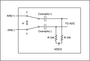
Figure 1. Fully-differential T / H stage.
In noisy environments, it is possible that coupled-noise could cause the differential inputs to exceed the ADC's allowable input voltage range. For best performance, reduce the input signal range to ensure that the ADC input range is not exceeded.
Another key advantage of differential signals is the increased dynamic range. With power supplies dropping to 3.3V and lower, design engineers are looking for ways to achieve greater input dynamic range. In theory, given the same voltage range for single-ended and fully- differential inputs, the fully-differential inputs will have double the dynamic range (Figure 2). This is because the two differential inputs can be 180 ° out of phase, as shown in Figure 3.
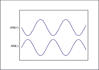
Figure 2. Single-ended vs. fully-differential.
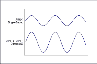
Figure 3. AIN (+) and AIN (-) 180 ° out of phase.
Another way to think about this is in relation to signal-to-noise ratio (SNR). The SNR is defined in terms of the ADC's full-scale input level and the minimum detectable signal:
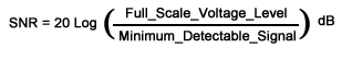 The minimum detectable signal is typically limited by the noise floor. Since fully-differential inputs have 2 times the full-scale input voltage level and have superior DC and AC common-mode rejection (which manifest themselves as noise), SNR increases. Floating Differential InputsIdeally, common-mode voltages beyond GND and VDD can exist in a differential system, provided that the differential voltage does not exceed the ADC input range. In practice, this is achievable only if the sensor and the ADC are isolated. In Figure 4's example , the voltages at AIN (+) and AIN (-) fall within the input range specified by the ADC, but a large common-mode voltage on the sensor output voltage forces the ADC inputs to exceed the maximum input voltage specification.
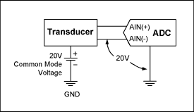
Figure 4. High common-mode voltage.
Figure 5 shows the same system, but using a separate power supply with galvanically isolated grounds. RBias biases the inputs to VREF / 2 to minimize drift due to leakage currents. As long as isolation between the grounds exists, the ADC only sees the differential voltage between AIN (+) and AIN (-), thus the transducer (or ADC) is referred to as "floating". (Note: To ensure galvanic isolation, all leakage paths between the transducer ground and system ground must be considered. A battery -powered system inherently provides isolation, provided its chassis is isolated from its internal ADC system ground).
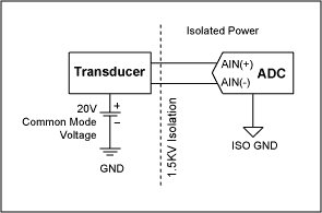
Figure 5. High common-mode voltage with a separate system power supply. Pseudo-Differential Inputs Pseudo-differential inputs are similar to fully-differential inputs in that they separate signal ground from the ADC ground, allowing DC common-mode voltages to be canceled ( unlike single-ended inputs). However, unlike fully-differential inputs, they have little effect on dynamic common-mode noise.
In Figure 6, sampling only occurs on the input AIN (+) signal. The signal common, AIN (-), is not sampled. During the 'TRACK' mode, the sampling capacitor charges through the series resistor RON. During the 'HOLD 'mode, the sampling capacitor connects to AIN (-) and an inverted input signal is presented to the ADC for conversion. Because sampling only occurs on the AIN (+) input, AIN (-) must remain within ± 0.1LSB during the conversion for optimal performance.
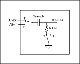
Figure 6. Pseudo-differential T / H stage.
An alternate method of implementing pseudo-differential inputs samples AIN (+) and AIN (-) sequentially, and the difference of the two voltages is provided as the conversion result.
For dynamic signals, the phase of AIN (+) and AIN (-) will not match during sampling resulting in distortion. Select an ADC with fully-differential inputs for dynamic time-varying signals.
A typical application for pseudo-differential inputs is measuring sensors that are biased to an arbitrary DC level. Some parts, like the MAX146, have a COM pin that allows single-ended inputs referenced to the common-mode voltage, making it pseudo-differential . All input channels are referenced to the COM voltage.
Figure 7 shows a thermistor connected in a Wheatstone-bridge application. In this example, AIN (+) and AIN (-) are both non-zero. The output code of the ADC will be a function of the differential voltage, AIN (+ )-AIN (-). The pseudo-differential inputs cancel out the DC common-mode voltage. To ensure AIN (-) is stable to within ± 0.1LSB, bypass AIN (-) to analog ground with a 0.1µF capacitor.
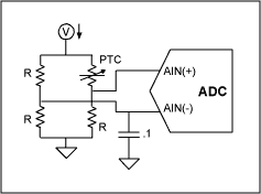
Figure 7. Wheatstone bridge application. Single-Ended Inputs Single-ended inputs are generally sufficient for most applications. In single-ended applications, all signals are referenced to a common ground at the ADC. Each channel uses a single input pin. The analog ground pin is shared between all inputs for multi-channel systems. DC offset and / or noise in the signal path will decrease the dynamic range of the input signal. Single-ended inputs are ideal if the signal source and ADC are close to each other ( ie, on the same board so that signal traces can be kept as short as possible). Single-ended inputs are more susceptible to coupled-noise and DC offsets. However, signal conditioning circuitry can reduce these effects.
Figure 8 shows a simplified example of a track-and-hold (T / H) input of a single-ended ADC. The sampling capacitor is switched to the input pin through a series resistance during the 'TRACK' mode. The switch opens when the T / H enters 'HOLD' mode (during the actual conversion process) and the ADC converts the voltage across the sampling capacitor into a digital code.
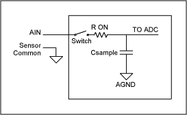
Figure 8. Single-ended T / H stage. Common-Mode Voltage and Common-Mode Rejection Ratios Common-mode voltage refers to a common voltage (ie, with the same magnitude and phase that appears on both differential inputs (Figure 9)). Common-mode rejection ratio (CMRR) is often specified for fully-differential inputs and describes the ADCs ability to reject a common-mode (typically DC) voltage. A DC common-mode voltage appearing across an ADC input has the same effect as a DC input offset. Normally, the sensor signal and ground wire are in close proximity physically and will couple in common-mode noise. The largest source of common-mode noise is often 50 / 60Hz noise from power lines. Power supply ripple, EMF, RF or high-frequency switching noise can also be sources of common-mode noise.
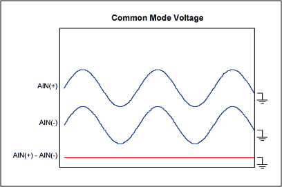
Figure 9. Common-mode voltage.
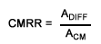
Common-mode rejection ratio (CMRR) is generally defined as the ratio between the differential voltage gain versus the common-mode voltage gain:
 Where:
 ADIFF = differential voltage gain
ACM = common-mode voltage gain
For ADCs, the differential voltage gain (ADIFF) is defined as ΔOutput_Code / ΔDifferential_Voltage and the common-mode voltage gain is defined as ΔOutput_Code / ΔCommon_Mode_Voltage. For fully-differential inputs, output code change will be small with respect to the common-mode voltage ; therefore the CMRR will be large and is often expressed on a logarithmic scale.
It is important to note that CMRR is a dependant on frequency-dependent parameter. As the frequency of the common-mode voltage increases, the phase matching between AIN (+) and AIN (-) for optimal common-mode rejection becomes more difficult to sustain. As a result, common-mode rejection is less effective at high frequencies. SummaryInterfacing a sensor to an ADC requires matching the sensor / signal conditioning output with the ADC input. Voltage output sensors provide either a single-ended or differential output. For single-end signals, all the inputs are referenced to system ground. Differential signals provide a positive and a negative signal with the positive output (AIN +) referenced to the negative output (AIN-).
Three common ADC input structures accommodate single-ended or differential output sensors: single-ended, pseudo-differential or fully-differential. The simplest method is to use a single-ended ADC when measuring single-ended signals. If a differential ADC is used to measure single-ended signals, simply connect the ADC AIN (-) pin to analog ground. This allows both single-ended and differential signals to be measured using a multi-channel differential input ADC.
Differential inputs can offer a performance improvement over single-ended inputs by measuring the difference in voltage between the positive and negative terminals of the sensor. This provides common mode rejection. Choose pseudo-differential ADCs for DC common-mode voltage rejection. For sensors requiring excitation, using pseudo-differential ADCs can zero out the bias voltages and allow the sensor ground to be different then the analog ground. Pseudo-differential inputs do not provide AC common-mode rejection. For dynamic common-mode rejection, choose fully-differential ADCs. Fully-differential inputs offer the best performance by rejecting DC and dynamic common-mode voltages. The final choice of which input structure to use will depend on the sensor, the signal conditioning circuitry, the application and the accuracy requirement.
Win 3 Flood Light BAT86 is applicable with different lamps and power(max 250 W),
LED: 60W/90W/120W/160W/200W/250W
Housing with Copper-free aluminium (yellow RAL1021) and toughened glass cover, stands 4J impact, can be used in Zone1 and Zone2,Zone 21 and Zone22
Flood light BAT86 can be setup with 3 ways: â‘ Mounted on the wall as wall light/garage light/garden light or Fixed with the ground spike as lawn light/landscape light/signage light. â‘¡Movable type, used in construction sites that require a lot of flexibility and mobility, like mining, tunnel projects oil field, railway construction.Set it as the stree lampâ‘¢ Street lamp type
Flood Light
Led Floodlight,Outdoor Flood Lights,Solar Led Flood Lights,Gas Monitor
ZHEJIANG HUACAI OPTIC-TECHNOLOGY CO LTD , https://www.win3safety.com