There are two signals involved in the superposition: live video signal and superimposed graphic signal. Since it is only required to complete the superimposition of the image acquired by the camera and reproduce the image on the monitor, the superimposed signal can be black level and white level. The black level is more obvious on the visual effect, so we choose to superimpose the black level. This "two choose one" switch can be realized by MAX442 produced by American MAXIM company. The MAX442 chip is a two-way video switch with an amplifier.It has a unity gain bandwidth of 140MHz and a conversion rate of 250V / μs; the phase error is less than 0.09 °, and the gain error is less than 0.07%; the channel switching rate is 36ns, which can directly drive 50Ω or 75Ω coaxial cable. Although its price is relatively expensive, considering the selection of it, the performance of the system can be greatly improved, and the overall cost of this project is still very low, that is, the price-performance ratio is reasonable, so this chip was chosen.
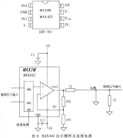
The pin diagram and connection circuit of MAX442 are shown in Figure 6. The capacitance value unit in the figure is μF, and the resistance unit is Ω. INO, IN1 are the input terminals of the two video signals, which are respectively connected to the live video signal and the black level; the address line AO ​​controls the "two choose one" switch to select which channel signal is output. AO occupies only one space in the screen editing buffer, so the superimposed control word can be read, written and modified bit by bit, which greatly reduces the storage space of the screen editing buffer RAM required. The data in RAM is accessed according to bytes, so when outputting, the data read from RAM needs to be converted into parallel to serial and sent to the AO end of MAX442. This kind of "eight-for-one" digital logic circuit can be easily realized with the programmable chip GAL, and the cost is not high, so we choose to use GAL to implement, and the logic expression is omitted.
Control design of screen editing buffer
The RAM used for the screen editing buffer is selected because the user requests to overlay regular geometric figures, and the algorithm for dynamically calculating the position of each point of the graph by the CPU 90C32 is very simple; the user can fully accept it.
Both the CPU and the video output have access to the screen editing buffer, where the CPU has to refresh the RAM, that is, "write" the RAM; the output only needs to read the RAM. That is to say, the access to RAM can be defined as "prohibit reading while writing" and "prohibit writing while reading". Let them share the data bus DB and the address bus AB, and use the time-sharing by controlling the enable terminal E of the address latch of the CPU and the field counter. It can be seen that the enable terminals E of these two sets of address latch buffers are mutually exclusive. You can use only one PI port I / O line of 90C32 to make a "single pole double throw switch", which is controlled by the CPU. / O line to realize the time-sharing use of the bus. Therefore, in the circuit design, the chip select terminal CS of the RAM is directly grounded, the write enable terminal WR is connected to the WR of the CPU, and the read enable terminal OE is connected to the enable terminal E of the address latch of the line / field counter. When the CPU wants to write to the screen editing buffer, the enable terminal E of its address latch is selected, and the address latch of the line counter is disabled, and the read enable terminal of the RAM is also disabled, that is, the RAM is in "Write only" status. On the contrary, when the CPU does not need to refresh the RAM, the enable terminal E of the address latch of the strobe line / field counter, and the read enable of the RAM are also gated, the RAM is in the "read" state, and write operations are prohibited. With this "memory dual-bus technology", conflicting access to the screen editing buffer is avoided, thereby ensuring data integrity and obtaining stable and correct superimposed video images.
The typical expansion circuit of the CPU 90C32 includes the expansion of the program storage area, the expansion of the data storage area, the expansion of the clock circuit and the crystal oscillator circuit. Taking into account the needs of the project and reserve some room for expansion, the memory ROM selects 27256 chips, and the RAM selects 61256 chips. Among them, except RAM (screen editing buffer) as the critical section, which requires special design, the other circuits are exactly the same as the general single-chip expansion circuit, and will not be introduced here.
2.4 Button decoding circuit
In this project, the user only needs four buttons when selecting the shape and size of the overlay cursor through human-computer interaction. Therefore, it is not necessary to use the powerful 8279 chip and directly extend the 90C32. The four buttons are decoded and sent to the P1 port of 90C32. This decoding logic is very simple, also implemented in GAL, and the logical expressions are omitted. In actual use, after the user selects the size and shape of the cursor once, it will always be stable for a period of time to perform its main work, so the time for operating the keys is very short for the working time of the entire system. The CPU responds to the button by using the interrupt method, which can greatly reduce the occupation of CPU processor resources than the polling method. In the button circuit, a total of 2 I / O lines on the P1 port are occupied. AO and A1 are the decoded button address (or code); and INT is an interrupt signal line to detect whether a button is pressed. External interrupt input  Connected. Usually INT is high level, if a key is pressed, INT is low level, CPU can respond to interrupt.
The design of the key circuit is also realized by a simple, typical and reliable universal circuit. At present, the button is operated by closing and breaking of the mechanical contact. When the electrical signal passes through the button, there is a jitter process at the moment of closing and opening. A series of negative pulses will appear, and the duration is generally 5 ~ 10ms . The stable closing period of the key is determined by the operator's key action, and it is generally a few tenths to a few seconds. In order to ensure that the CPU closes the key once, only one key input process is performed, and the influence of jitter must be removed. Generally, there are two kinds of measures to affect the debounce: hardware and software. This project uses double debounce to improve reliability: In hardware design, add a capacitor connected to the ground at the input end for each button to filter out glitch pulses; software design There is a key debounce process, the specific ideas are described in detail in the software design.
8 Layer PCB - Stackup & Cost & Prototype manufacture
What is 8 layer PCB?
The 8 layer PCB is a circuit board with 8 layers that are stacked firmly together with predefined and dependable mutual connections between the layers. Structure of eight layer PCB is more complicated. Nowadays, PCBs frequently have 8 to 12 layers or more, and electronics engineers know that designing for so many layers requires a well-configured layer stack.
8-layer Printed Circuit Boards are usually installed in compact equipment with strict spacing requirements, such as notebook computer motherboard, communication backplane, wearable watches, etc. Because of its complexity and high manufacturing costs, your 8-layer PCB Manufacturing should be made by reliable and experienced manufacturers. Jinghongyi PCB has been specially targeting high-end PCB manufacturing and assembly services for 8 years, providing high-quality products and services for various customers. Our advanced production line and fast response team will keep you comfortable and reassured, without any trouble, you can rest assured to place the order with us.

Typical 8-layer PCB stack up methods and guidelines
Standard stackup of 8 layer PCB looks as follows
- Signal1
- Ground
- Signal2
- Power
- Ground
- Signal3
- Power
- Signal4
Eight-layer PCB can be used to add two additional layers, or two planes can be added to improve EMC performance. Most eight-layer circuit boards are superimposed to improve EMC performance, rather than adding additional wiring layers. Compared with 6-layer circuit boards, the cost increase percentage of 8-layer PCB is less than that of 4-layer PCB to 6-layer PCB. Therefore, in order to improve EMC performance, the cost increase is reasonable. Therefore, most 8-layer boards consist of four wiring layers and four planes.

8 Layer PCB Stack up

8 Layer PCB stackup
In short, 8 layer PCB are usually used to improve the EMC performance of circuit boards, rather than increasing the number of layers.
No matter how you decide on the stack layer, it is not recommended to use an 8-layer PCB Board with six wiring layers. If you need six routing layers, you should use a 10 Layer PCB board. Therefore, the 8-layer board can be regarded as the six-layer board with the best EMC performance.
Basic Layer of Eight-Layer Circuit Board with Excellent EMC Performance

All signal layers are adjacent to the plane, and all layers are tightly coupled. High-speed signals are buried between planes, so planes provide shielding to reduce the transmission of these signals. In addition, the circuit board uses multiple grounding layers to reduce the grounding impedance.
Other forms of 8-layer PCB stackup

A typical 8 Layer PCB Stackup

0.062[8 layer PCB stackup

0.093[ 8-Layer PCB Stackup
So far, we have also clarified the cost and price differences between 6-layer PCB, 8-layer PCB and 10-layer PCB.
8 Layer PCB thickness

8 LAYER 1.6 MM STANDARD STACKUP AND THICKNESS
8 Layer Stackup - 1.6mm thickness |
||||||
| layer order | layer name | material type | material description | dielectric constant | thickness | copper weight |
| 1 | top | copper | signal | 0.035mm | 1 oz | |
| 2116 | prepreg | 4.5 | 0.12mm | |||
| 2 | inner 1 | copper | plane | 1 oz | ||
| core | 4.6 | 0.3mm | ||||
| 3 | inner 2 | copper | plane | 1 oz | ||
| 7630 | prepreg | 4.7 | 0.2mm | |||
| 4 | inner 3 | copper | plane | 1 oz | ||
| core | 4.6 | 0.3mm | ||||
| 5 | inner 4 | copper | plane | 1 oz | ||
| 7630 | prepreg | 4.7 | 0.2mm | |||
| 6 | inner 5 | copper | plane | 1 oz | ||
| core | 4.6 | 0.3mm | ||||
| 7 | inner 5 | copper | plane | 1 oz | ||
| 2116 | prepreg | 4.5 | 0.12mm | |||
| 8 | bottom | copper | signal | 0.035mm | 1 oz | |
| Final board thickness: 1.6mm±0.13mm | ||||||
8-Layer Prototype PCB Manufacturing Service
The 8-layer prototype FR-4 PCB is an 8-layer circuit board, which is firmly stacked together with predefined and reliable interconnection between layers. The 8-layer FR-4 PCB has more complex structure. Jinghongyi PCB is a large enterprise located in Shenzhen, China, which can manufacture 8-layer prototype PCB.
Jinghongyi PCB can provide you with multi-layer PCB board in accordance with RoHS standard. With laminated material, it can match high temperature in assembly process. Importantly, some lead-free assembly processes will require laminated substrates to withstand temperatures exceeding 260 degrees Celsius or 500 degrees Fahrenheit over a longer period of time. To solve this problem, we have high temperature laminates in stock, so that our customers can meet the higher temperature cycle requirements of some lead-free assembly applications.
JHY PPCB is one of the leading 8 layer PCB manufacturers. For more information, pls send email to us.

8 Layer PCB
PCB Circuit Board,8 Layer PCB,Custom multilayer pcb,Custom 8 Layer PCB
JingHongYi PCB (HK) Co., Limited , https://www.pcbjhy.com