Abstract: This applicaTIon note is designed to assist in the use of the DS1020 / DS1021 programmable delay lines. The basic principles of device operaTIon are covered in simplified form, but with sufficient detail to enable the user to understand what is happening within the device and how this affects its use in pracTIcal applicaTIons. These flexible devices can be configured as traditional delay lines, as pulse width modulators or even as programmable oscillators. A variety of configurations are illustrated, the various features of which cover most applications. Some of the key considerations which must be taken into account when designing in these products, based on the experience of previous users of the devices, are also covered.
IntroductionThis application note is designed to assist in the use of the DS1020 / DS1021 programmable delay lines. The basic principles of device operation are covered in simplified form, but with sufficient detail to enable the user to understand what is happening within the device and how this affects its use in practical applications.
These flexible devices can be configured as traditional delay lines, as pulse width modulators or even as programmable oscillators. A variety of configurations are illustrated, the various features of which cover most applications.
Some of the key considerations which must be taken into account when designing in these products, based on the experience of previous users of the devices, are also covered.
The DS1020 / DS1021 are similar devices, differing only in package and step size availability and response to power-up conditions.
Key Product Features Programmable over 256 steps in increments of 0.15 to 2ns (DS1020), 0.25 or 0.5ns (DS1021) Guaranteed monotonicity Serial (3-wire) or parallel (8-bit) programmability Cascadable DIP (DS1020 only) or SOIC packaging Product Selection (all times in ns)
Circuit Configurations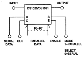
Programmable Delay Line
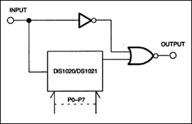
Programmable Pulse Width
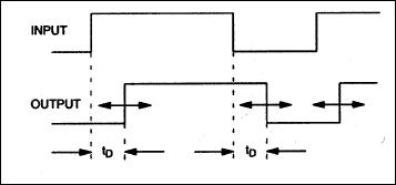
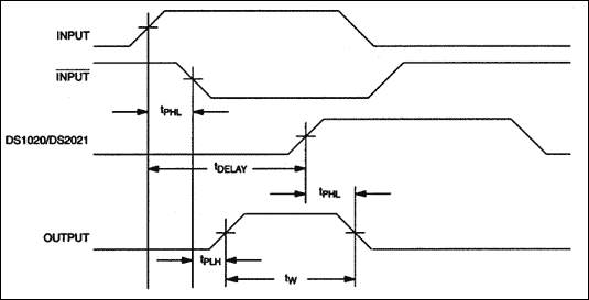
Figure 1. Timing waveforms.
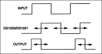
Figure 2. Output waveforms.
This is the "normal" mode of operation for the DS1020 / DS1021. Input pulses applied to the device reappear at the output after a delay time set by the device programming. Both leading and trailing edges of the input waveform are delayed by the same amount .
The delay time can be programmed either by means of a serial data input or can be loaded into an 8-bit parallel port. A Mode Select pin (S) determines which mode of operation is to be used. An Enable pin is available to latch in the serial data once it has been loaded, or to load parallel data and isolate the device from further changes to a shared parallel bus.
NOTE: In some of the following applications control and / or data input pins have been omitted for clarity. Unless reference is made to specific inputs, the same configuration can be used in either the serial or parallel mode.
The DS1020 / DS1021 can be combined with some simple external logic to produce a programmable pulse width. In the example shown above the output pulse is triggered by the rising edge of the input waveform and can be adjusted in duration from 10ns (the latent delay of the DS1020 / DS1021) up to the maximum programmed delay value.
For correct operation over the full range of desired output pulse widths, the duration of both the high and low states of the input must be greater than the delay time of the DS1020 / DS1021 which corresponds to the maximum output pulse width.
The rising edge of the output will be delayed with respect to the input by the propagation delay through the two gates. The falling edge will be dependent on the programmed delay of the DS1020 / DS1021 and the propagation delay of the output gate (see diagram next page).
Therefore the output pulse width is given by:

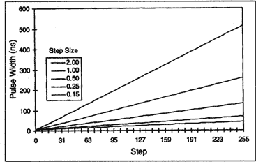
Figure 3. Pulse width modulator.
Figure 3 shows the range of pulse widths available for the various members of the DS1020 / DS1021 family.
NOTE: Using HCMOS gates the minimum pulse width will be approximately 5ns.
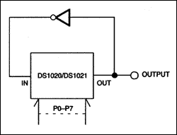
Programmable OscillatorIf the output of the DS1020 / DS1021 is inverted and fed back to the input, a free-running oscillator is produced. The oscillator can be gated if desired by replacing the inverter with a NAND or NOR function and using the additional input as an enable.
The period of the output signal will equal approximately twice the sum of the programmed delay and the propagation delay through the inverter, or more accurately:


The minimum frequency is determined by the maximum achievable delay from the DS1020 / DS1021, the maximum is determined by the propagation delay of the inverter and the step 0 delay time of the DS1020 / DS1021.
The following table summarizes some bench measurements on three of the available speed options:
In practice the speeds tend to be higher than suggested by the data sheet values ​​for the inverter propagation delays because the devices are more lightly loaded.
The maximum frequency can be increased by using a faster inverter:
The jitter values ​​shown in these charts are approximate values ​​for the peak to peak jitter on the output signal. The effect of jitter increases as the operating frequency is increased, but can be minimized by device decoupling.
The increased jitter of the oscillator using an HCMOS inverter versus an F-TTL inverter can be attributed to the difference in noise coupled to the supply when the inverter output changes state. The HCMOS "through current" results in a larger glitch on the supply than the bipolar totem-pole output stage.
Using this bench data we can project the performance for each member of the family across its entire programming range. Figures 4 and 5 show the theoretical frequencies obtainable for given programmed delay values. The first chart assumes an HCMOS type inverter or gate, the second achieves a greater maximum frequency by using an F-TTL device.
To derive these charts the following values ​​have been used for the propagation delays of the inverters:

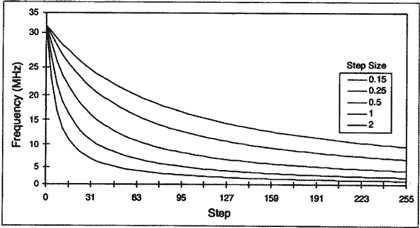
Figure 4. Frequency Vs. programmed step (HCMOS inverter).
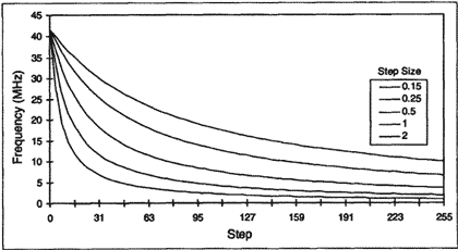
Figure 5. Frequency Vs. programmed step (F-TTL inverter).
Closed Loop OperationAny of the preceding configurations can also be set up for closed loop operation. In this mode some sort of feedback loop is set up such that the programming pins are modified until the output delay, or some other parameter dependent on the output delay, reaches a desired level or state. The advantage of this arrangement is that the negative feedback eliminates any effects caused by device error (deviation between actual delay and programmed delay).
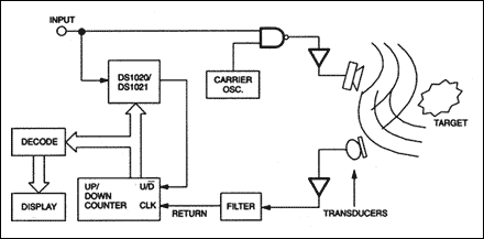
Figure 6. Ultrasonic rangefinder application.
A digital ultrasonic rangefinder is shown to illustrate the use of the DS1020 / DS1021 in a closed loop mode. These devices can be used in a variety of ultrasound, laser and video applications and with a variety of feedback mechanisms. For example in laser applications an analog feedback loop with an AID could be used to control pulse energy or power, for mouse pointer applications the feedback is provided by the operator moving a mouse until the pointer is located at the desired location.
In the example shown an input waveform is used to generate a series of ultrasonic bursts which are emitted by a transducer.
This signal gates an oscillator (at the appropriate carrier frequency), which results in a burst duration equal to the high level pulse width of the input and a burst frequency dependent on the period of the carrier oscillator.
If a target is present the signal will be reflected to the receiver, which can be amplified and have the carrier removed to leave a return pulse that will be delayed from the input signal by an amount dependent on the distance to the target.
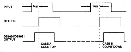
Figure 7. Timing waveforms.
To measure this distance the programmed delay of the DS1020 / DS1021 is adjusted until it matches the delay of the RETURN pulse. This is done by using the rising edge of the return pulse to increment or decrement an up / down counter, while the direction of count is governed by the state of the DS1020 / DS1021 output. In the diagram above Case A shows too small a delay from the DS1020 / DS1021, the output is high so the clock pulse from the return signal will cause the counter to increment. In Case B the delay is too large, so in this case the output is low and the clock pulse will cause the counter to decrement. Eventually, when the DS1020 / DS1021 delay time approximately equals the return delay, a state will be reached where the counter alternately decrements and increments on each cycle.
The resulting programmed value can then be decoded and displayed (including conversion from programmed value to distance dimensions and, if greater accuracy is wanted, corrections for device error).
Performance LimitationsWhile this example serves to illustrate the principle it does show some performance limitations which render it unsuitable for a practical application.
When the programmed delay is approximately equal to the return delay the LSB of the counter will toggle, therefore it is probably advisable to discard the LSB from the displayed value to keep it stable.
The response time of the system is also somewhat slow as the counter is only incremented or decremented by one count each cycle, so many cycles may be needed before the delays are matched. Some additional gating of the return signal, the DS1020 / DS1021 output and a high frequency clock could be used to allow the counter to count up or down multiple clock cycles, depending on the timing difference between the return signal and the DS1020 / DS1021 output.
Cascading Multiple DevicesMultiple devices can be simply cascaded together. When this is done the input to output delay will be equal to twice (or n times for n devices) the step 0 delay (20ns) plus the sum of the programmed delays for each device. This is equivalent to doubling the number of steps, or range, of a single device.
Figure 8 shows the arrangement for serial programming. The serial data output is daisy chained to the serial input of the following device, and the clock and enable pins are connected and driven in parallel. The Mode Select pin (S) is tied low for serial operation. (The unused parallel data pins, PI-P7, must be tied to a well defined logic level and not allowed to float.)
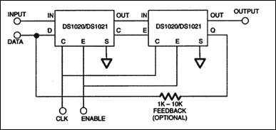
Figure 8. Serial operation.
Also shown is a feedback resistor to allow the contents of the internal registers to be read back. If this option is used the source driving the serial data input must be in a high impedance state during readback.
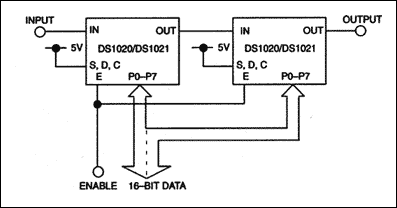
Figure 9. Parallel operation—16 bit.
If parallel programming is preferred the parallel data inputs (P0-P7) are driven, the Mode Select pin (S) is held high, and the unused serial data in (D) and clock (C) pins are tied to well defined logic levels . In this mode the Enable pin can be permanently tied high, or driven to a low level to latch in the programmed data and allow further changes on the data inputs to be ignored (eg, for use on a data bus).
In the parallel mode the data could be 16-bits wide, or two 8-bit bytes could be used with the Enable pins on each device being driven separately to steer each byte of data to the appropriate device.
If the data lines for each device are driven in parallel (both Enables high) it is functionally equivalent to having a single DS1020 / DS1021 with twice the delay step size and total delay. The same effect can be realized in the serial mode either by driving the data inputs (D) in parallel (do not connect the Q output from the first device to the D input of the second!) or by simply repeating the same 8-bit sequence twice in the daisy chain mode (see Figure 10).
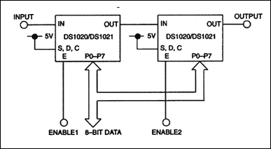
Figure 10. Parallel operation—8 bit.
Principles Of OperationThis section gives some insight into what is happening internally to the device. While it is not necessary to review this to use the device, it is beneficial when it comes to understanding some of the design considerations discussed in this brief.
Basic Delay Element
The diagram above shows the basic delay line timing element. The input signal is effectively integrated by ramp generators which must exceed the comparator threshold voltage before the input pulse is transferred to the output via an SR latch. The positive-going edge of the input signal is used to initiate a timing ramp which ultimately sets the output latch; the negative-going edge of the input initiates a second ramp which ultimately will reset the latch.
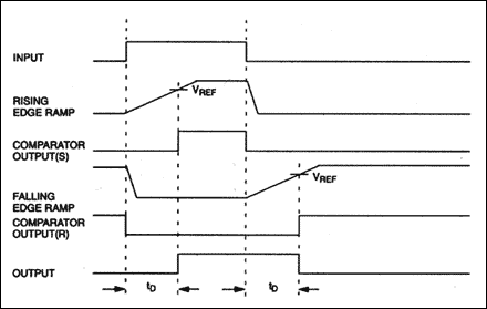
Figure 11. Timing waveforms.
Therefore, as can be seen from the timing diagrams, the delay time is dictated by the slope of the rising and falling edge ramp generators (assuming a fixed threshold voltage for the comparators).
Ramp Generators
The basic elements of the ramp generators are capacitors which are charged at a constant rate from programmable current generators. Prior to a timing period the capacitor is kept discharged by the input transistor. When an input transition occurs the input transistor is turned off, allowing the capacitor to charge up to the threshold voltage of the comparator, which in turn sets (or resets) the output latch. When the input returns to its original state, the input transistor discharges the capacitor ready for the next cycle.
NOTE: Inverter stages are inserted between the device input pin and the input transistor as appropriate for either the rising edge delay or the falling edge delay portions of the circuit.
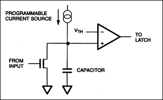
Programmable Current Source

A representation of the programmable current source is shown above. An internally derived reference voltage is applied to an array of resistors. The resistance of this array will therefore set the value of the current flowing through the output transistors. This current is in turn mirrored by another transistor in the ramp generator circuit.
The value of the resistor array is determined by the binary code applied to the digital inputs. This binary number is decoded and used to select the appropriate resistor combination to set the desired current. Laser trimming is employed during manufacture to minimize the effect of normal process variations on the accuracy of the resistor values.
Design ConsiderationsDelay Tolerance
An "ideal" programmable delay line would show a linear response between the programmed delay value and the measured output delay (see Figure 12). In the real world manufacturing variances, eg normal process tolerances, etc., result in a deviation from this ideal response. The charts on the following pages show typical response curves for members of the DS1020 / DS1021 family. This data is the average for five devices of each speed grade, and was taken at nominal conditions (5V supply and 25 ° C). The scales on the charts have been chosen such that the maximum and minimum values ​​correspond to the data sheet limits for deviation from the ideal response for each device.
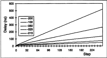
Figure 12. DS1020 / DS1021 "Ideal" response.
NOTE: There is an additional (tighter) tolerance specification for the step 0, or inherent, delay of the device.
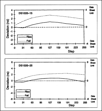
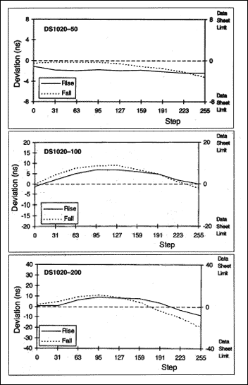
Figure 13. Deviation (ns).
The significance of this variation will depend on the application. In closed loop systems, as long as the programmed delay versus actual delay response is monotonic, the loop will settle to the correct value.
In systems where the delay is not altered during normal operation (only being changed during a production calibration step, for example), the programmed value can be varied until the desired measured delay is reached. This value can then be hardwired on the board, typically using DIP switches or jumpers.
Jitter
The output of the device is subject to some random fluctuations (jitter) caused by noise. This effect can be minimized by good supply voltage decoupling, but some jitter will remain due to internally generated noise. This effect is most noticeable at the longer programmed delays (when the internal charge currents are smallest), when a small amount of noise can cause some variation in the internal trigger points.
The following charts show some typical variations in peak-to-peak jitter with output delay for the various members of the family. When considered as a percentage of the programmed output delay the peak-to-peak jitter will usually be less than 3%.
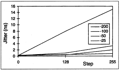
Figure 14. Peak-to-peak jitter (rising edge).
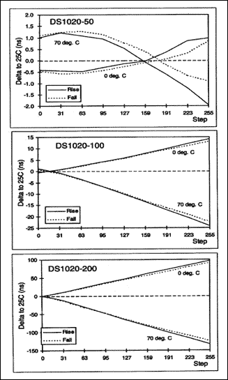
Figure 15. Peak-to-peak jitter (falling edge).
The actual measured peak-to-peak jitter will be very dependent on the actual circuit configuration (eg, noise on the supply, decoupling, other noise sources in close proximity, etc.). This probably accounts for the somewhat anomalous readings for the- 200 device rising edge. An rms measurement of jitter will yield somewhat smaller results. The main consideration is that output jitter will exist and that it will increase with longer programmed delays.
In the extreme situation when the input pulse width is close to the programmed delay value there can be a substantial increase in jitter. This is caused by noise being introduced to the supply line when the output changes state. If this noise occurs close to the next transition on the input, the trigger point becomes less well defined and output jitter will increase. Although the device should not normally be operated under these conditions, it is of interest when using configurations such as the oscillator described above, and explains why the jitter of the oscillator exceeds the values ​​shown above.
NOTE: If you wish to attempt to make jitter measurements it is unwise to simply measure the delay time between successive output edges. Most test generators also generate jitter. Therefore timing measurements should be made between an input edge and the corresponding output edge.
Improving Absolute Accuracy
Systems in which the delay is changed during operation and have no feedback applied may require a greater absolute accuracy than the data sheet tolerance, perhaps approaching the same magnitude as the individual step size. In this situation each device will need to be individually calibrated to the desired accuracy. Typically this would be done by measuring actual delay values ​​in the application and generating a look-up table in EPROM for use in normal operation.
Alternatively the device can be operated in a closed loop mode to eliminate the effects of any inaccuracies.
Output Loading
As with any type of delay line the output delay will be dependent on the output loading. The DS1020 / DS1021 is tested and characterized with a load of 15 pF. Different values ​​of load capacitance will change the slope of the output rise and fall waveforms and produce a resultant change in measured delay time.
The effect of various output loads can be approximated by assuming the output consists of a voltage source, switch and resistors as shown in this diagram:
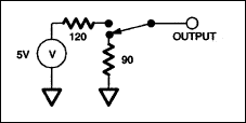
Figure 16. Simplified output model.
Using this model the following charts were generated to show the predicted change in output transition with load capacitance.
NOTE: The resistor values ​​used were chosen so that the charts approximate to actual (dynamic) in-circuit performance and do not necessarily apply for DC analysis.
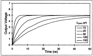
Figure 17. Output loading (low-to-high).
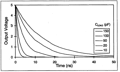
Figure 18. Output loading (high-to-low).
Voltage and Temperature Variations
The data sheet specifications on delay tolerance apply at 25 ° C and with a 5V supply. The DS1020 / DS1021 feature on-chip circuitry to minimize the effect of temperature changes, but there will still be some change in the resultant delays if either the temperature or supply voltage changes from these nominal values.
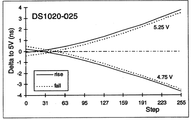
Figure 19. Supply voltage variation.
Supply Voltage Variation
The chart above shows the variation in delay time with supply voltage. It can be seen that the variation is almost directly proportional to the programmed value. The maximum variation is about 3.5ns for this device, which is approximately 5% of the programmed delay. This results from a 5% change in supply voltage, so a good approximation to the percentage change in delay can be obtained by assuming that it is equal to the percentage change in supply voltage.
Even though the data shown pertains to the -025 device, all the members of the family exhibit similar characteristics.
Temperature Variation
Some typical variations with temperature for the DS1020 / DS1021 family members are shown in the following charts. This data is based on a sample of five devices of each speed option, operating from a 5V supply. In each case the change in delay versus 25 ° C operation is indicated, where positive values ​​indicate an increased delay and negative numbers a decreased delay. Data was taken for both rising and falling edges and at the extremes of the operating temperature range.
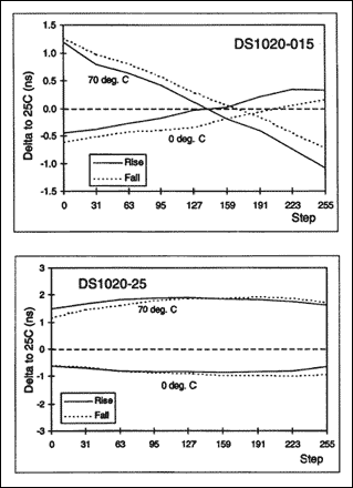
Figure 20. Delta to 25C (ns).
Power Up and Changing the Programmed Delay
Power Up
Changing the Programmed Delay
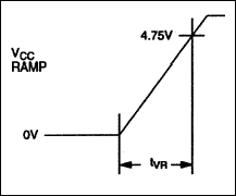
The DS1020 / DS1021 features internal Power-On Reset circuitry to ensure that all the internal functions are brought up in the correct state. However, if the supply voltage is brought up too rapidly, a situation can occur where the device does not have enough time to complete these reset activities before attempting to go into normal operation.
Most system power supplies come up relatively slowly and have no adverse effect on normal device operation. The DS1020 / DS1021 differ in their tolerance to rapidly rising supplies. The DS1021 will operate correctly when the rise time (tVR) is greater than 20 ms. An additional test screen for the DS1020 allows the use of faster rise times, down to approximately 2 ms.
If it becomes necessary to use either device with a power supply which rises too quickly to meet the respective rise time requirements, it may be possible to use a series resistance from the system supply to the device supply pin in conjunction with additional decoupling capacitance at the device. Care should be taken to ensure that the voltage applied to the device remains within the data sheet limits when the device supply and load currents are taken into account.
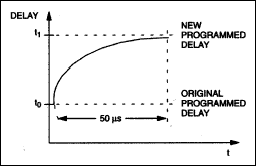
The data sheet contains two parameters, tVPD and tEDV, which relate to the time taken after a programming change before the output delay is valid. Some commonly asked questions are:
Why is this delay so long (50 µs)? What happens in the time until this condition is met? To understand the reason for this delay it is necessary to refer to the means by which the delay is programmed. The main reason is related to the programmable current source. When the programming is changed there is a finite settling time associated with the op amp configuration of the current source. Therefore the 50 µs is derived from the time taken for this current source to become stable at the new value.
While the current source is settling the device continues to operate normally—input pulses continue to be delayed before reappearing at the output. However, the exact duration of the delay will be uncertain until the settling time has passed. In practice, pulses arriving during this 50 µs time interval will typically be delayed by an amount somewhere between the old programmed value and the new programmed value. The current source settles in an exponential fashion and this is reflected by an exponential change in delay time until the new, stable value is reached .
Minimum Input Pulse Width / Period
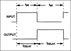
For the device to operate correctly the input pulse width must be greater than the output delay time (see diagram above). This applies to both the high level pulse width and the low level pulse width. The reason for this is that the input pulse is integrated to provide the output delay.
For example, consider the case when the input is in a high state. The leading edge ramp generator must be allowed to reach the comparator threshold, and set the output latch, before the input changes state. Otherwise the output will not go high, the leading edge ramp generator will be reset, and the trailing edge ramp will be initiated. In effect, the input pulse has been "swallowed."
NOTE: This phenomenon can be used to good effect as a pulse width discriminator. By selecting altering the programmed value only pulses widths greater than a certain value will be output, narrow pulses (and / or noise) will be rejected.
The tolerance of the output delay must also be taken into account and the input pulse widths set to exceed the maximum actual delay rather than the ideal programmed value.
From the preceding paragraph it can be seen that the minimum input period will be equal to twice the minimum pulse width (assuming a square wave input). The data sheet limit of three times the input pulse width is therefore somewhat conservative. As long as adequate margins are included to allow for device tolerances correct operation is assured.
Notes: If you are in need of further information, please contact:
Steve Brightman
Dallas Semiconductor
4401 South Beltwood Parkway,
Dallas, TX 75244-3292
Email: var name = "brightman @"; var domain = "dalsemi.com"; document.write ("" + name + domain + "");
Phone: 972 / 371-3865
Acknowledgments:
TK Hui and Rich Tarver for insights on the inner workings of the devices.
Sokhom Chum for the characterization work.
John Kuhfeldt for the lab assistance.
IntroductionThis application note is designed to assist in the use of the DS1020 / DS1021 programmable delay lines. The basic principles of device operation are covered in simplified form, but with sufficient detail to enable the user to understand what is happening within the device and how this affects its use in practical applications.
These flexible devices can be configured as traditional delay lines, as pulse width modulators or even as programmable oscillators. A variety of configurations are illustrated, the various features of which cover most applications.
Some of the key considerations which must be taken into account when designing in these products, based on the experience of previous users of the devices, are also covered.
The DS1020 / DS1021 are similar devices, differing only in package and step size availability and response to power-up conditions.
Key Product Features Programmable over 256 steps in increments of 0.15 to 2ns (DS1020), 0.25 or 0.5ns (DS1021) Guaranteed monotonicity Serial (3-wire) or parallel (8-bit) programmability Cascadable DIP (DS1020 only) or SOIC packaging Product Selection (all times in ns)
| Part Number | Step 0 Delay | Delay Per Step | Maximum Delay |
| DS1020-015 | 10 | 0.15 | 48.25 |
| DS1020-025 DS1021-025 | 10 | 0.25 | 73.75 |
| DS1020-050 DS1021-050 | 10 | 0.5 | 137.50 |
| DS1020-100 | 10 | 1 | 265.00 |
| DS1020-200 | 10 | 2 | 520.00 |
Circuit Configurations
Programmable Delay Line
Programmable Pulse Width
Figure 1. Timing waveforms.
Figure 2. Output waveforms.
This is the "normal" mode of operation for the DS1020 / DS1021. Input pulses applied to the device reappear at the output after a delay time set by the device programming. Both leading and trailing edges of the input waveform are delayed by the same amount .
The delay time can be programmed either by means of a serial data input or can be loaded into an 8-bit parallel port. A Mode Select pin (S) determines which mode of operation is to be used. An Enable pin is available to latch in the serial data once it has been loaded, or to load parallel data and isolate the device from further changes to a shared parallel bus.
NOTE: In some of the following applications control and / or data input pins have been omitted for clarity. Unless reference is made to specific inputs, the same configuration can be used in either the serial or parallel mode.
The DS1020 / DS1021 can be combined with some simple external logic to produce a programmable pulse width. In the example shown above the output pulse is triggered by the rising edge of the input waveform and can be adjusted in duration from 10ns (the latent delay of the DS1020 / DS1021) up to the maximum programmed delay value.
For correct operation over the full range of desired output pulse widths, the duration of both the high and low states of the input must be greater than the delay time of the DS1020 / DS1021 which corresponds to the maximum output pulse width.
The rising edge of the output will be delayed with respect to the input by the propagation delay through the two gates. The falling edge will be dependent on the programmed delay of the DS1020 / DS1021 and the propagation delay of the output gate (see diagram next page).
Therefore the output pulse width is given by:
Figure 3. Pulse width modulator.
Figure 3 shows the range of pulse widths available for the various members of the DS1020 / DS1021 family.
NOTE: Using HCMOS gates the minimum pulse width will be approximately 5ns.
Programmable OscillatorIf the output of the DS1020 / DS1021 is inverted and fed back to the input, a free-running oscillator is produced. The oscillator can be gated if desired by replacing the inverter with a NAND or NOR function and using the additional input as an enable.
The period of the output signal will equal approximately twice the sum of the programmed delay and the propagation delay through the inverter, or more accurately:
The minimum frequency is determined by the maximum achievable delay from the DS1020 / DS1021, the maximum is determined by the propagation delay of the inverter and the step 0 delay time of the DS1020 / DS1021.
The following table summarizes some bench measurements on three of the available speed options:
| Device | Step Size | Step Number | Frequency | Jitter (ns) |
| DS1020-025 | 0.25ns | 255 128 0 | 5.8 9.7 33.0 | 5.0 2.0 1.0 |
| DS1020-100 | 1ns | 255 128 0 | 1.8 3.2 33.0 | 10.0 5.0 1.5 |
| DS1020-200 | 2ns | 255 128 0 | 0.9 1.7 30.0 | 22.0 14.0 1.5 |
In practice the speeds tend to be higher than suggested by the data sheet values ​​for the inverter propagation delays because the devices are more lightly loaded.
The maximum frequency can be increased by using a faster inverter:
| Device: DS1020-025 | Step Size: 0.25ns | |||
| Step Number | 'HC04 | 'F04 | ||
| Frequency (MHz) | Jitter (ns) | Frequency (MHz) | Jitter (ns) | |
| 255 | 5.8 | 5.0 | 6.5 | 2.5 |
| 128 | 9.7 | 2.0 | 10.8 | 1.2 |
| 0 | 33.0 | 1.0 | 47.0 | 0.3 |
The jitter values ​​shown in these charts are approximate values ​​for the peak to peak jitter on the output signal. The effect of jitter increases as the operating frequency is increased, but can be minimized by device decoupling.
The increased jitter of the oscillator using an HCMOS inverter versus an F-TTL inverter can be attributed to the difference in noise coupled to the supply when the inverter output changes state. The HCMOS "through current" results in a larger glitch on the supply than the bipolar totem-pole output stage.
Using this bench data we can project the performance for each member of the family across its entire programming range. Figures 4 and 5 show the theoretical frequencies obtainable for given programmed delay values. The first chart assumes an HCMOS type inverter or gate, the second achieves a greater maximum frequency by using an F-TTL device.
To derive these charts the following values ​​have been used for the propagation delays of the inverters:
Figure 4. Frequency Vs. programmed step (HCMOS inverter).
Figure 5. Frequency Vs. programmed step (F-TTL inverter).
Closed Loop OperationAny of the preceding configurations can also be set up for closed loop operation. In this mode some sort of feedback loop is set up such that the programming pins are modified until the output delay, or some other parameter dependent on the output delay, reaches a desired level or state. The advantage of this arrangement is that the negative feedback eliminates any effects caused by device error (deviation between actual delay and programmed delay).
Figure 6. Ultrasonic rangefinder application.
A digital ultrasonic rangefinder is shown to illustrate the use of the DS1020 / DS1021 in a closed loop mode. These devices can be used in a variety of ultrasound, laser and video applications and with a variety of feedback mechanisms. For example in laser applications an analog feedback loop with an AID could be used to control pulse energy or power, for mouse pointer applications the feedback is provided by the operator moving a mouse until the pointer is located at the desired location.
In the example shown an input waveform is used to generate a series of ultrasonic bursts which are emitted by a transducer.
This signal gates an oscillator (at the appropriate carrier frequency), which results in a burst duration equal to the high level pulse width of the input and a burst frequency dependent on the period of the carrier oscillator.
If a target is present the signal will be reflected to the receiver, which can be amplified and have the carrier removed to leave a return pulse that will be delayed from the input signal by an amount dependent on the distance to the target.
Figure 7. Timing waveforms.
To measure this distance the programmed delay of the DS1020 / DS1021 is adjusted until it matches the delay of the RETURN pulse. This is done by using the rising edge of the return pulse to increment or decrement an up / down counter, while the direction of count is governed by the state of the DS1020 / DS1021 output. In the diagram above Case A shows too small a delay from the DS1020 / DS1021, the output is high so the clock pulse from the return signal will cause the counter to increment. In Case B the delay is too large, so in this case the output is low and the clock pulse will cause the counter to decrement. Eventually, when the DS1020 / DS1021 delay time approximately equals the return delay, a state will be reached where the counter alternately decrements and increments on each cycle.
The resulting programmed value can then be decoded and displayed (including conversion from programmed value to distance dimensions and, if greater accuracy is wanted, corrections for device error).
Performance LimitationsWhile this example serves to illustrate the principle it does show some performance limitations which render it unsuitable for a practical application.
When the programmed delay is approximately equal to the return delay the LSB of the counter will toggle, therefore it is probably advisable to discard the LSB from the displayed value to keep it stable.
The response time of the system is also somewhat slow as the counter is only incremented or decremented by one count each cycle, so many cycles may be needed before the delays are matched. Some additional gating of the return signal, the DS1020 / DS1021 output and a high frequency clock could be used to allow the counter to count up or down multiple clock cycles, depending on the timing difference between the return signal and the DS1020 / DS1021 output.
Cascading Multiple DevicesMultiple devices can be simply cascaded together. When this is done the input to output delay will be equal to twice (or n times for n devices) the step 0 delay (20ns) plus the sum of the programmed delays for each device. This is equivalent to doubling the number of steps, or range, of a single device.
Figure 8 shows the arrangement for serial programming. The serial data output is daisy chained to the serial input of the following device, and the clock and enable pins are connected and driven in parallel. The Mode Select pin (S) is tied low for serial operation. (The unused parallel data pins, PI-P7, must be tied to a well defined logic level and not allowed to float.)
Figure 8. Serial operation.
Also shown is a feedback resistor to allow the contents of the internal registers to be read back. If this option is used the source driving the serial data input must be in a high impedance state during readback.
Figure 9. Parallel operation—16 bit.
If parallel programming is preferred the parallel data inputs (P0-P7) are driven, the Mode Select pin (S) is held high, and the unused serial data in (D) and clock (C) pins are tied to well defined logic levels . In this mode the Enable pin can be permanently tied high, or driven to a low level to latch in the programmed data and allow further changes on the data inputs to be ignored (eg, for use on a data bus).
In the parallel mode the data could be 16-bits wide, or two 8-bit bytes could be used with the Enable pins on each device being driven separately to steer each byte of data to the appropriate device.
If the data lines for each device are driven in parallel (both Enables high) it is functionally equivalent to having a single DS1020 / DS1021 with twice the delay step size and total delay. The same effect can be realized in the serial mode either by driving the data inputs (D) in parallel (do not connect the Q output from the first device to the D input of the second!) or by simply repeating the same 8-bit sequence twice in the daisy chain mode (see Figure 10).
Figure 10. Parallel operation—8 bit.
| Enable1 | Enable2 | OPERATION |
| 0 | 0 | Data latched into both devices. Changes on data bus have no effect. |
| 0 | 1 | Data latched in device 1. Device 2 follows data bus. |
| 1 | 0 | Data latched in device 2. Device 1 follows data bus. |
| 1 | 1 | Both devices follow data bus. Equivalent to single device with 2x step size and range. |
Principles Of OperationThis section gives some insight into what is happening internally to the device. While it is not necessary to review this to use the device, it is beneficial when it comes to understanding some of the design considerations discussed in this brief.
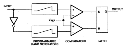
Basic Delay Element
The diagram above shows the basic delay line timing element. The input signal is effectively integrated by ramp generators which must exceed the comparator threshold voltage before the input pulse is transferred to the output via an SR latch. The positive-going edge of the input signal is used to initiate a timing ramp which ultimately sets the output latch; the negative-going edge of the input initiates a second ramp which ultimately will reset the latch.
Figure 11. Timing waveforms.
Therefore, as can be seen from the timing diagrams, the delay time is dictated by the slope of the rising and falling edge ramp generators (assuming a fixed threshold voltage for the comparators).
Ramp Generators
The basic elements of the ramp generators are capacitors which are charged at a constant rate from programmable current generators. Prior to a timing period the capacitor is kept discharged by the input transistor. When an input transition occurs the input transistor is turned off, allowing the capacitor to charge up to the threshold voltage of the comparator, which in turn sets (or resets) the output latch. When the input returns to its original state, the input transistor discharges the capacitor ready for the next cycle.
NOTE: Inverter stages are inserted between the device input pin and the input transistor as appropriate for either the rising edge delay or the falling edge delay portions of the circuit.
Programmable Current Source
A representation of the programmable current source is shown above. An internally derived reference voltage is applied to an array of resistors. The resistance of this array will therefore set the value of the current flowing through the output transistors. This current is in turn mirrored by another transistor in the ramp generator circuit.
The value of the resistor array is determined by the binary code applied to the digital inputs. This binary number is decoded and used to select the appropriate resistor combination to set the desired current. Laser trimming is employed during manufacture to minimize the effect of normal process variations on the accuracy of the resistor values.
Design ConsiderationsDelay Tolerance
An "ideal" programmable delay line would show a linear response between the programmed delay value and the measured output delay (see Figure 12). In the real world manufacturing variances, eg normal process tolerances, etc., result in a deviation from this ideal response. The charts on the following pages show typical response curves for members of the DS1020 / DS1021 family. This data is the average for five devices of each speed grade, and was taken at nominal conditions (5V supply and 25 ° C). The scales on the charts have been chosen such that the maximum and minimum values ​​correspond to the data sheet limits for deviation from the ideal response for each device.
Figure 12. DS1020 / DS1021 "Ideal" response.
NOTE: There is an additional (tighter) tolerance specification for the step 0, or inherent, delay of the device.
Figure 13. Deviation (ns).
The significance of this variation will depend on the application. In closed loop systems, as long as the programmed delay versus actual delay response is monotonic, the loop will settle to the correct value.
In systems where the delay is not altered during normal operation (only being changed during a production calibration step, for example), the programmed value can be varied until the desired measured delay is reached. This value can then be hardwired on the board, typically using DIP switches or jumpers.
Jitter
The output of the device is subject to some random fluctuations (jitter) caused by noise. This effect can be minimized by good supply voltage decoupling, but some jitter will remain due to internally generated noise. This effect is most noticeable at the longer programmed delays (when the internal charge currents are smallest), when a small amount of noise can cause some variation in the internal trigger points.
The following charts show some typical variations in peak-to-peak jitter with output delay for the various members of the family. When considered as a percentage of the programmed output delay the peak-to-peak jitter will usually be less than 3%.
Figure 14. Peak-to-peak jitter (rising edge).
Figure 15. Peak-to-peak jitter (falling edge).
The actual measured peak-to-peak jitter will be very dependent on the actual circuit configuration (eg, noise on the supply, decoupling, other noise sources in close proximity, etc.). This probably accounts for the somewhat anomalous readings for the- 200 device rising edge. An rms measurement of jitter will yield somewhat smaller results. The main consideration is that output jitter will exist and that it will increase with longer programmed delays.
In the extreme situation when the input pulse width is close to the programmed delay value there can be a substantial increase in jitter. This is caused by noise being introduced to the supply line when the output changes state. If this noise occurs close to the next transition on the input, the trigger point becomes less well defined and output jitter will increase. Although the device should not normally be operated under these conditions, it is of interest when using configurations such as the oscillator described above, and explains why the jitter of the oscillator exceeds the values ​​shown above.
NOTE: If you wish to attempt to make jitter measurements it is unwise to simply measure the delay time between successive output edges. Most test generators also generate jitter. Therefore timing measurements should be made between an input edge and the corresponding output edge.
Improving Absolute Accuracy
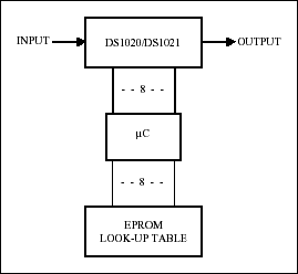
Systems in which the delay is changed during operation and have no feedback applied may require a greater absolute accuracy than the data sheet tolerance, perhaps approaching the same magnitude as the individual step size. In this situation each device will need to be individually calibrated to the desired accuracy. Typically this would be done by measuring actual delay values ​​in the application and generating a look-up table in EPROM for use in normal operation.
Alternatively the device can be operated in a closed loop mode to eliminate the effects of any inaccuracies.
Output Loading
As with any type of delay line the output delay will be dependent on the output loading. The DS1020 / DS1021 is tested and characterized with a load of 15 pF. Different values ​​of load capacitance will change the slope of the output rise and fall waveforms and produce a resultant change in measured delay time.
The effect of various output loads can be approximated by assuming the output consists of a voltage source, switch and resistors as shown in this diagram:
Figure 16. Simplified output model.
Using this model the following charts were generated to show the predicted change in output transition with load capacitance.
NOTE: The resistor values ​​used were chosen so that the charts approximate to actual (dynamic) in-circuit performance and do not necessarily apply for DC analysis.
Figure 17. Output loading (low-to-high).
Figure 18. Output loading (high-to-low).
Voltage and Temperature Variations
The data sheet specifications on delay tolerance apply at 25 ° C and with a 5V supply. The DS1020 / DS1021 feature on-chip circuitry to minimize the effect of temperature changes, but there will still be some change in the resultant delays if either the temperature or supply voltage changes from these nominal values.
Figure 19. Supply voltage variation.
Supply Voltage Variation
The chart above shows the variation in delay time with supply voltage. It can be seen that the variation is almost directly proportional to the programmed value. The maximum variation is about 3.5ns for this device, which is approximately 5% of the programmed delay. This results from a 5% change in supply voltage, so a good approximation to the percentage change in delay can be obtained by assuming that it is equal to the percentage change in supply voltage.
Even though the data shown pertains to the -025 device, all the members of the family exhibit similar characteristics.
Temperature Variation
Some typical variations with temperature for the DS1020 / DS1021 family members are shown in the following charts. This data is based on a sample of five devices of each speed option, operating from a 5V supply. In each case the change in delay versus 25 ° C operation is indicated, where positive values ​​indicate an increased delay and negative numbers a decreased delay. Data was taken for both rising and falling edges and at the extremes of the operating temperature range.
Figure 20. Delta to 25C (ns).
Power Up and Changing the Programmed Delay
Power Up
Changing the Programmed Delay
The DS1020 / DS1021 features internal Power-On Reset circuitry to ensure that all the internal functions are brought up in the correct state. However, if the supply voltage is brought up too rapidly, a situation can occur where the device does not have enough time to complete these reset activities before attempting to go into normal operation.
Most system power supplies come up relatively slowly and have no adverse effect on normal device operation. The DS1020 / DS1021 differ in their tolerance to rapidly rising supplies. The DS1021 will operate correctly when the rise time (tVR) is greater than 20 ms. An additional test screen for the DS1020 allows the use of faster rise times, down to approximately 2 ms.
If it becomes necessary to use either device with a power supply which rises too quickly to meet the respective rise time requirements, it may be possible to use a series resistance from the system supply to the device supply pin in conjunction with additional decoupling capacitance at the device. Care should be taken to ensure that the voltage applied to the device remains within the data sheet limits when the device supply and load currents are taken into account.
The data sheet contains two parameters, tVPD and tEDV, which relate to the time taken after a programming change before the output delay is valid. Some commonly asked questions are:
Why is this delay so long (50 µs)? What happens in the time until this condition is met? To understand the reason for this delay it is necessary to refer to the means by which the delay is programmed. The main reason is related to the programmable current source. When the programming is changed there is a finite settling time associated with the op amp configuration of the current source. Therefore the 50 µs is derived from the time taken for this current source to become stable at the new value.
While the current source is settling the device continues to operate normally—input pulses continue to be delayed before reappearing at the output. However, the exact duration of the delay will be uncertain until the settling time has passed. In practice, pulses arriving during this 50 µs time interval will typically be delayed by an amount somewhere between the old programmed value and the new programmed value. The current source settles in an exponential fashion and this is reflected by an exponential change in delay time until the new, stable value is reached .
Minimum Input Pulse Width / Period
For the device to operate correctly the input pulse width must be greater than the output delay time (see diagram above). This applies to both the high level pulse width and the low level pulse width. The reason for this is that the input pulse is integrated to provide the output delay.
For example, consider the case when the input is in a high state. The leading edge ramp generator must be allowed to reach the comparator threshold, and set the output latch, before the input changes state. Otherwise the output will not go high, the leading edge ramp generator will be reset, and the trailing edge ramp will be initiated. In effect, the input pulse has been "swallowed."
NOTE: This phenomenon can be used to good effect as a pulse width discriminator. By selecting altering the programmed value only pulses widths greater than a certain value will be output, narrow pulses (and / or noise) will be rejected.
The tolerance of the output delay must also be taken into account and the input pulse widths set to exceed the maximum actual delay rather than the ideal programmed value.
From the preceding paragraph it can be seen that the minimum input period will be equal to twice the minimum pulse width (assuming a square wave input). The data sheet limit of three times the input pulse width is therefore somewhat conservative. As long as adequate margins are included to allow for device tolerances correct operation is assured.
Notes: If you are in need of further information, please contact:
Steve Brightman
Dallas Semiconductor
4401 South Beltwood Parkway,
Dallas, TX 75244-3292
Email: var name = "brightman @"; var domain = "dalsemi.com"; document.write ("" + name + domain + "");
Phone: 972 / 371-3865
Acknowledgments:
TK Hui and Rich Tarver for insights on the inner workings of the devices.
Sokhom Chum for the characterization work.
John Kuhfeldt for the lab assistance.
For lithium iron phosphate(LiFePO4) power battery system with brand of Taihang Jiaxin, it has the advantages of long cycle life, high rate of discharge performance, good safety, available for the requirement for Fast Charging and so on.
Using self-developed Battery Management System (BMS) which has the functions of advanced battery self-management, communication, alarm and other functions.

Lifepo4 Battery Pack,Lifepo4 Battery Pack 12V,24V Lifepo4 Battery Pack,48V Lifepo4 Battery Pack
Xinxiang Taihang Jiaxin Electric Tech Co., Ltd , https://www.chargers.be