&, developed and mass-produced Wicop LEDs , overcoming the imperfections of CSPs caused by silicon semiconductors.
&, do not need brackets, gold wire and other traditional packaging materials necessary for the main components of materials and solid crystal, gold wire and other packaging equipment.
& With the commercialization of Wicop, the burden of led companies that have invested heavily in packaging engineering will gradually increase.
&, has obtained the international patent portfolio related to Wicop and is concerned about the trend of imitating products.

Seoul Semiconductor representative Lee Min Hoh showcases new products
On September 15th, Seoul Semiconductor (representative director: Li Yixun), an international LED professional company, announced at the Marriott Hotel in Pudong, Shanghai, China that Die Bonding, which is completely eliminating the need for LED package, is Wire Bonding. In addition, there is no need for a new concept of Wicop LED, a new concept of materials such as lead frames and gold wires, which are the main components of LED packages.

Wicop2 new product for lighting (Z8Y15 with length and width of 1.5mm
Wicop (Wafer Level Integrated Chip On PCB) is a new concept LED product that breaks through the current CSP (Chip Scale Package) and truly realizes the unpackaged LED. It was the first in the world by Seoul Semiconductor in 2012. Successfully developed and mass produced. Since the chip is directly connected to the PCB, there is no need for the die bonding (Wire Bonding) and the like required by the conventional LED packaging process, and the chip size is the same as the package size by 100% because there is no intermediate substrate. It is an ultra-small, high-efficiency product that exhibits extremely high optical density and thermal conductivity.
The traditional LEDs currently used in the market need to use Die Bonding, Wire Bonding and other engineering equipment to fix the chip on the special bracket, and also need to purchase the bracket, gold wire, and bonding. Materials such as agents. The size of LED package products manufactured by this conventional packaging process is much larger than that of chips, and there are certain limitations in miniaturization of products.
At the same time, CSP (Chip Scale Package), which is derived from silicon semiconductor technology, is a technology that reduces the area of ​​semiconductor components (components) to the size of a chip. Generally, if the size of the package does not exceed 1.2 times the size of the chip. , is divided into CSP. This technology has been applied by the LED industry. In 2012, P products and other products were published. However, the product using this technology cannot be regarded as a perfect packageless LED because it uses a die bonder and a ceramic/silicon intermediate substrate in order to fix the chip on the PCB.
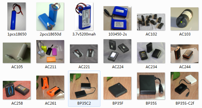
We make all types of 3.7 volt battery, 3v Battery, 3.5v battery, 3.6v battery for battery heated gloves, warmest womens gloves, heated glove liners, heated ski gloves, heated mittens, warmest mittens, warmest ski gloves, heated gloves and socks, usb heated gloves, battery operated gloves, electric geated gloves, heated motorclycles gloves, rechargeable battery heated gloves, battery powered heated gloves, heated sneaks, heated insoles, warm boots, heated boot, heated insoles, ski boot insoles, heated shoes.

3V Heated Socks Battery,Heated Socks Battery, Foot Warmers Battery,Heated Insole Battery
Asarke Industry Co., Limited , https://www.asarke-industry.com