The system is a wireless identification system based on the principle of digital communication and integrated with a single-chip narrow-band UHF transceiver. The basic working principle and hardware design idea of ​​the radio frequency identification system are expounded, and the flow chart of the program design scheme is given. Design RFID tags for vehicles from low power, efficient identification and practical perspective. The test results show that the system can effectively identify within 300m under the condition of complex road conditions (busy road surface), and can effectively identify up to 500 m under line-of-sight conditions.
The Internet of Things refers to real-time collection of any monitoring and control through various information sensing devices, such as sensors, radio frequency identification (RFID) technology, global positioning systems, infrared sensors, laser scanners, gas sensors and other devices and technologies. Connected, interactive objects or processes, collecting a variety of information required by sound, light, electricity, biology, location, etc., combined with the Internet to form a huge network. Its purpose is to realize the connection between objects and objects, objects and people, all items and networks, and to facilitate identification, management and control. This project focuses on the key issues of data acquisition, transmission and application in the vehicle Internet of Things, and designs a new generation of vehicle-mounted RFID systems based on short-range wireless RF communication technology. The system consists of a short-range wireless communication unit (OBU) and a base station system (BSS) to form a point-to-multipoint wireless identification system (WIS), which can be used in the coverage of the base station. Vehicle identification and intelligent guidance.
1 system hardware design
The system hardware is mainly composed of a control part, a radio frequency part and an external extended application part. The low-power MCU is used as the control unit to integrate the single-chip narrow-band UHF transceiver with built-in optimized antenna design. Powered by advanced photovoltaic cells, the highly integrated short-range wireless identification radio terminal (OBU). The terminal is small in size, low in power consumption, wide in scope, and has an open protocol and standard interface for easy connection with existing systems or other systems.
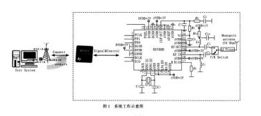
The system works as shown in Figure 1.
1.1 Control circuit design
The control unit uses the MSP430 series produced by TI, a relatively low-power application in the industry. This series is a 16-bit ultra-low-power mixed-signal processor (Mired Signal Proessor) that TI introduced to the market in 1996. Application requirements integrate many analog circuits, digital circuits, and microprocessors on a single chip to provide a "single-chip" solution. In the WIS system, the working principle is the same in the OBU and the BSS, so the design of the OBU part is mainly introduced, and the schematic diagram of the control part is shown in Fig. 2.
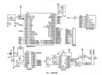
The input voltage of MSP430F2274 is 1.8~3.6V. When operating at a clock of 1 MHz, the power consumption of the chip is around 200 to 400 μA, and the minimum power consumption of the clock shutdown mode is only 0.1 μA. Since the function modules opened during system operation are different, three different working modes of standby, running and hibernation are adopted, which effectively reduces the system power consumption.
The system uses two clock systems; the basic clock system and the Digitally Controlled Oscillator (DCO), which uses an external crystal oscillator (32 768 Hz). After the power-on reset, the MCU (Microprogrammed Control Unit) is first started by DCOCLK to ensure that the program starts from the correct position, ensuring sufficient oscillation and stabilization time of the crystal oscillator. The software can then set the control bits of the appropriate registers to determine the final system clock frequency. If the crystal oscillator fails when used as the MCU clock MCLK, the DCO will automatically start to ensure normal operation of the system; if the program runs away, it can be reset by the watchdog. This design uses the on-chip peripheral module watchdog (WDT), analog comparator A, timer A (Timer_A), timer B (Timer_B), serial USART, hardware multiplier, 10-bit / 12-bit ADC, SPI bus, etc. .
1.2 RF circuit
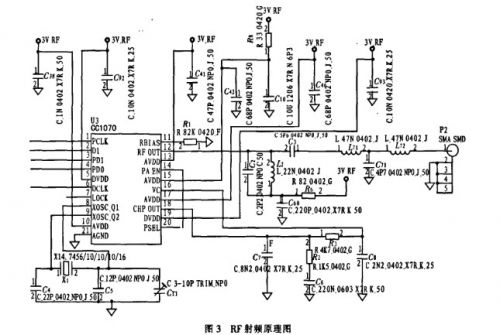
The RF part adopts TI's CC1020 as the RF control unit. This chip is the industry's first true single-chip narrowband UHF transceiver with FSK/GFSK/OOK three modulation modes. The minimum channel spacing is 50 kHz, which can meet multiple channels. Strict requirements for narrowband applications (402-470 MHz and 804-94O MHz bands), multiple operating bands can be switched freely, operating voltage 2.3 to 3.6 V, ideal for integration into mobile devices as wireless data transmission or electronics The label is used. The chip complies with EN300 220. ARIB STD-T67 and FCC CFR47 part15 specifications.
The carrier frequency of 430 MHz is selected as the working frequency band. This frequency band is the ISM frequency band and conforms to the national wireless management committee standard, and no frequency is required. Using FSK modulation mode, it has high anti-interference ability and low error rate. It adopts forward error correction channel coding technology to improve the ability of data to resist burst interference and random interference. The channel error rate is 10-2. At this time, the actual bit error rate is 10-5 to 10-6. The data transmission distance can reach 800 m in open field-of-sight conditions, baud rate 2A Kbs, large suction cup antenna (length 2m, gain 7.8 dB from ground level 2m). The standard configuration of the RF chip provides 8 channels to meet multiple communication combinations. Communication stability and anti-interference are enhanced due to the narrowband communication technology. The schematic diagram of the RF part is shown in Figure 3.
1.3 system power supply
The system power supply part is powered by a photovoltaic battery as a daily working power supply and a lithium sub-battery as a backup battery. Under the condition of good illumination, the energy storage battery is charged by solar energy, and the guaranteed illumination time can meet the daily working needs of the OBU, greatly prolonging the service life of the backup battery and prolonging the working life of the OBU. Suitable for vehicles that are often used outdoors, it can collect enough sunlight for photovoltaic cells to work.
1.4 System Development Environment
The system development environment is as follows: 1) IAR Embedded Workbench for MSP430 compiler; 2) PADS PCB Design Solutions 2007 Beth board design tool.
LED Outdoor wall Light is one of the categories of outdoor lamps. Outdoor Wall Light can play the role of illumination in the outdoors. Outdoor wall light not only has very strong appreciation , but also illume effect concentrates. However,outdoor wall light is contracted, be aware of not easily, can improve people to article visual effect again . Outdoor Wall Lights are used in corridors and corridors. Outdoor wall lights are auxiliary lighting fixtures installed on walls.
Outdoor Wall Light
Outdoor Sconces,Led Wall Lights Outdoor,Outdoor Wall Lanterns,Outdoor Wall Sconces
JIANGMEN LEDERLIGHT LIGHTING Co.,LTD , https://www.lederlightcn.com