Due to the market's need to improve the performance of information technology and communication equipment, today's system designers face the enormous challenge of designing EMI-compatible products. Prior to sale, all information technology equipment (ITE), which are usually specified to have a modulated clock signal above 9 kHz, must meet relevant government standards, such as FCC Part 15 Subpart B in the United States and EN55022 in the European Union, which stipulate industrial and commercial Maximum allowable radiated emissions from the environment (ClassA) and the home environment (ClassB). In view of such strict EMI standards, engineering human resource constraints and rapid product launch requirements, the penetration rate of power modules certified by the EN55022 standard has increased. However, it is important to know the electrical operating conditions of the power module at the time of certification to avoid surprises in the subsequent design process. An understanding of the EMI sources and field strength factors in switch-mode regulators will help design engineers select the best components to mitigate electromagnetic emissions, especially in state-of-the-art devices that require higher current levels.
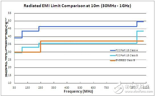
Figure 1: FCC Radiation Limits (USA) and EN55022 Class B Radiation Limits (EU)
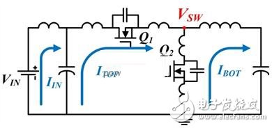
Figure 2: Step-Down Switching Regulator with Parasitic Inductors and Capacitors
Due to its special nature, switching power supplies generate electromagnetic waves that radiate into the surrounding atmosphere. The pulse voltage and current will appear due to the switching action and directly affect the intensity of the radiated electromagnetic wave. In addition, parasitic devices inside the converter also generate electromagnetic radiation. Figure 2 shows a typical buck converter that includes parasitic inductors and parasitic capacitors for the power MOSFET.
EMI radiation source
During each switching cycle, the energy stored in the parasitic inductor will resonate with the energy stored in the parasitic capacitor. When the energy is released, a large voltage spike is generated at the switching node (VSW), which is up to twice the input voltage, as shown in Figure 3. As the current capability of the MOSFET increases, the energy stored in the parasitic capacitor tends to increase. In addition, the switching action also pulses the input current and the current flowing through the top MOSFET (ITOP) and the bottom MOSFET (IBOT). This pulsed current will generate electrical waves on the input power cable and the PCB board trace (which acts as the transmit antenna), producing both radiated and conducted emissions.
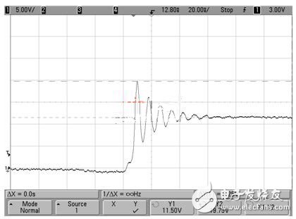
Figure 3: Typical Switch Node Voltage Spikes and Ringing in a 12V Input Step-Down Switching Regulator
As the input voltage and output current increase, the voltage spike on the switch node will also increase as the power inductor changes polarity in each cycle. Moreover, the higher the output current, the larger the pulse current generated inside the circuit loop. Therefore, the radiation emission depends to a large extent on the electrical operating conditions in which the device under test is located. In general, radiated noise will increase as the input voltage and output power (especially the output current) increase. Because linear regulators, which are low-noise alternatives, are too inefficient and dissipate too much heat at high voltages and high power levels, designers have to overcome the challenges of adopting state-of-the-art switching power solutions. Among them, EMI suppression has become quite tricky.
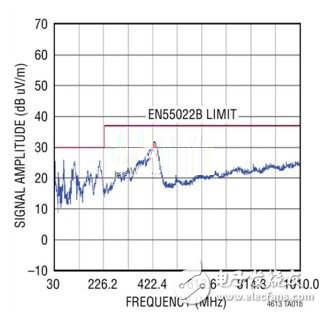
Figure 4: EN55022 Standard Conformance Demonstration of LTM4613 (DC1743) at 96W Output Power (implemented by an independent test facility)
EMI suppression
Alternative approaches to reducing radiated EMI from switch mode power converter designs present other challenges. One conventional approach is to add an EMI shield around the power solution that will contain an EMI field within the metal enclosure. However, EMI shielding increases design complexity, size, and cost. Routing an RC damper circuit on the switch node (VSW) helps reduce voltage spikes and subsequent ringing. However, adding a damper circuit will reduce the operating efficiency, thereby increasing power dissipation, resulting in an increase in ambient temperature and PCB temperature. The last countermeasure is to adopt an excellent PCB layout scheme, including the use of local low ESR ceramic decoupling capacitors, and a short PCB trace spacing for all high current paths to minimize the parasitic effects shown in Figure 2. , but at the cost of increased engineering time and delays in the launch of the product. In general, in order to meet both size, efficiency, heat dissipation and EMI specifications, engineers must have extensive power supply design experience and make difficult trade-offs, especially in high input voltage, high output power applications (reasons) As mentioned above). In order to evaluate trade-off strategies and design a power converter that meets EMI standards and meets all system requirements, circuit designers often need to spend a lot of time and effort. Guaranteed EMI-compliant solutions
In order to guarantee a simple and EMI-compliant high-output power supply design, Linear Technology submitted the LTM46138A step-down μModule regulator demo board (DC1743) to an independent certification test lab (TUVRheinland). The laboratory's 10-meter EN55022 test chamber was officially recognized by the US National Institute of Standards and Technology (US NaTIonal InsTItute of Standards and Technology NIST). In the case of a 24V input providing 96W output power, the LTM4613 demo board was found to meet the EN55022 ClassB limit. A worry-free solution to EN55022 can be easily implemented with input capacitors, output capacitors and a small number of other small components, especially when using the free downloadable DC1743 Gerber file. under.
The LTM4613 offers the highest output power and efficiency in all commercially available power module products that are certified to EN55022B. With a carefully designed integrated filter, detailed internal layout, shielded inductors, internal snubber circuits and power transistor drivers, the LTM4613 provides the perfect balance between size, output power, efficiency and EMI emissions. The LTM4613 and many other members of the EN55022B-certified μModule regulator family (which have various output power levels) eliminate the need for additional magnetic shields and external dampers, reducing overall solution size and cost. And some troublesome design tasks.
to sum up
Designing information technology equipment (ITE) products for EMI compliance is an inevitable requirement that requires extraordinary skill and time. Although cumbersome, such limitations are critical to ensuring proper functioning of adjacent electronic devices or other accessory components within the system itself. To meet this demand, the industry has introduced power modules such as the LTM4613 that are certified to EN55022 Class B. However, since the EMI field strength depends to a large extent on many factors (eg input voltage, output current, output voltage and PCB layout), it should be determined when comparing products: EN55022 certification is under similar electrical conditions Conducted (an industry-recognized EMI test lab implemented at input voltages and output power levels similar to your design). Linear Technology has published EMI test results and demonstration board illuminating files for the most common working conditions, providing a good power supply design certified by an authorized independent laboratory, which gives customers a "reassuring".
Fiber Optic Distribution Box / Fiber Splitter Box is used as a termination point for the feeder cable to connect with drop cable. The fiber splicing, splitting, distribution can be done in this box, and meanwhile it provides solid protection and management for the FTTX network building.
Material: PC+ABS,wet-proof, water-proof, dust-proof, anti-aging, protection grade is IP65.
Small Volume, For Indoor/Outdoor application. Compact structure,convenient installation and maintenance.


Fiber Optical Distribution Box (Plastic)
Fiber Optical Distribution Box,Plastic Fiber Optical Distribution Box,Fiber Optic Distribution Box,Optical Distribution Boxes
Sijee Optical Communication Technology Co.,Ltd , https://www.sijee-optical.com