Abstract: In wireless communications, reducing the phase noise of a frequency synthesizer and suppressing its corresponding parasitic output has always been the goal pursued by designers. PE3293 is a high-performance 1.8GHz / 550MHz dual-mode integer frequency division integrated phase-locked loop circuit produced by Peregrine, which has ultra-low parasitic output. The article introduces the characteristic function and composition principle of PE3293, and gives the application circuit of PE3293 in the design of frequency synthesizer.
1 Introduction
In wireless applications, phase noise and parasitic output are key parameters of the frequency synthesizer. The RF system design of phase modulation cellular systems such as PHS, GSM and IS-54 requires low-noise frequency synthesis modules. 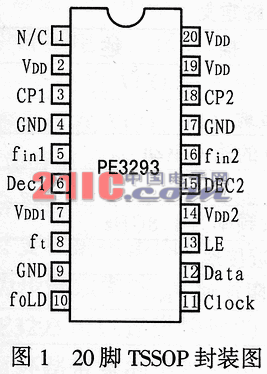 At the same time, the frequency switching time and the suppression of the parasitic output are also very important to the system. As a high-quality signal source, the frequency synthesizer has a great relationship with the performance of the electronic system. In communication systems, the use of highly stable signal sources can make full use of frequency resources. In fact, in electronic systems such as electronic countermeasures and navigation, high-index signal sources will bring good cost performance to the system, thereby providing reliable technical support for system designers.
There are three methods of frequency synthesis: direct, phase-locked and direct digital. Among them, the direct frequency synthesis method is rarely used because the output harmonics, noise and spurious frequency are difficult to suppress; the currently widely used direct digital frequency synthesis method also faces two difficulties: the difficulty of raising the upper limit of the output frequency and the difficulty of suppressing the parasitic output. The phase-locked frequency synthesizer is the result of the development and application of phase-locked technology in the 1970s. With the increasing degree of integration, various digital circuits such as various control circuits, program dividers, frequency / phase detectors, etc. It can now be integrated into a chip. Therefore, now, many microwave and millimeter wave frequency synthesizer designs often use phase-locked frequency synthesis methods to achieve.
2 Features of PE32293
2.1 Main features
PE3293 is a high-performance 1.8GHz / 550MHz dual-mode integer frequency division integrated phase-locked loop produced by Peregrine. It integrates a pulse shaping circuit, frequency discrimination / phase discrimination circuit, pre-frequency division, program frequency divider, ÷ 32/33 and ÷ 16/17 two dual-mode frequency dividers, control circuits and phase-locked indication circuits. Because the IC uses Pergrine's UTSi CMOS patented technology, its parasitic output components are extremely low throughout the operating band. PE32293 has the following characteristics:
â— Using advanced parasitic output suppression technology, it has very good phase noise characteristics and high frequency stability;
◠With ÷ 32/33 and ÷ 16/17 two dual-mode frequency dividers? Among them the working frequency of the former can reach 1.8GHz, the latter can reach 500MHz; 
â— The power consumption is very small, when the dual-ring working mode is adopted, the typical working current is 4mA;
◠Working voltage is 2.7 ~ 3.3V;
â— It has two packages: 24-pin BCC and 20-pin TSSOP;
â— Can be used in PCS base stations, CDMA and handheld wireless products.
2.2 Pin description
PE32293 has two packages as shown in Figure 1 and Figure 2? Among them, the 24-pin BCC package only has 4 more reserved pins than the 20-pin TSSOP package, and the pin definitions of the other pins are the same. The 20 pins listed in Table 1 Pin definition of TSOP package.
Table 1 Pin definition of PE3293 (Take 20-pin TSSOP package as an example)
| No. | Name | Types of | Function description |
| 1 | N / C | Not connected | |
| 2 | VDD | Power supply, 2.7 ~ 3.3V, need a capacitor to bypass ground nearby | |
| 3 | CP1 | Output | Pulse shaping output inside PLL1, used as input drive for external VCO |
| 4 | GND | Ground | |
| 5 | fin1 | Input | Prescaler input from PLL1 (RR) VCO, the maximum frequency is 1.8GHz |
| 6 | Dec1 | PLL1 power supply decoupling terminal, it is necessary to use a capacitor to ground | |
| 7 | VDD1 | The power supply of the PLL1 prescaler is generally connected to VDD via a 3.3kΩ resistor | |
| 8 | fr | Input | Reference frequency input |
| 9 | GND | Ground | |
| 10 | f0LD | Output | Multiplexer output, including PLL1 and PLL2 main counter or reference counter output / clock detection signal, and shift register to shift out data |
| 11 | Clock | Input | CMOS clock input, on the rising edge of the clock signal, serial data of various counters will be sent to the 21bit shift register |
| 12 | Data | Input | Binary serial data input, CMOS input data, MSB first, 2bit LSB is control bit |
| 13 | LE | Input | The load enables CMOS input. When LE is high, the data word in the 21bit serial shift register will be sent to one of the corresponding four latches (determined by the control bit) |
| 14 | VDD2 | Output | The power supply of the PLL1 prescaler is connected to VDD0 through a 3.3kΩ resistor when in use |
| 15 | Dec2 | Output | PLL1 power supply decoupling terminal, it is necessary to use a capacitor to ground |
| 16 | fin2 | Input | Prescaler input from PLL1 (IF) VCO, the maximum frequency is 500MHz |
| 17 | GND | Ground | |
| 18 | CP2 | Output | Pulse shaping output inside PLL1, used as input drive for external VCO |
| 19 | VDD | 2.7 ~ 3.3V power supply, need to be grounded nearby through a capacitor | |
| 20 | VDD | Power supply, 2.7 ~ 3.3V, need to be grounded nearby through a capacitor |
3 Composition principle of PE32293
The functional block diagram of PE32293 is shown in Figure 3. It is mainly composed of 21-bit serial control register, a multiplexer and phase-locked loops PLL1 and PLL2. Each PLL has a set of integer main counters divided by N, a reference counter, a phase discriminator and an internal pulse shaper with internal compensation circuits, and each integer main counter divided by N includes an internal dual-mode prescaler It can be used as counting and decimal accumulation.
The data input from the serial data input terminal Data can be shifted into the 21-bit shift register one by one on the rising edge of the clock. Among them, MSB? M16? Is input first. When LE is high, the data is sent to the last 2 address bits The corresponding address of the 21bit shift register. Figure 4 shows the register bits of PE32293. If fLD is used as a data output, the content of S20 in the shift register will be sent to fLD on the falling edge of the CLOCK, so that PE32293 and the corresponding device form a ring structure. 
The VCO frequency fin1 of PL1 (RF) is related to the value of fr, and the relationship between them is as follows:
fin1 = [(32 & TImes; M1) + A1 + (F1 / 32)] & TImes;? fr / R1?
It is worth noting that in order to obtain continuous channels, A1 must be less than or equal to M1, and fin1 must be greater than or equal to 1024 times (fr / R1).
The VCO frequency fin2 of PL2 (IF) is related to the value of fr, and their relationship is as follows:
fin2 = [16M2 + A2 + (F2 / 32)] & TImes; (fr / R2)
Similarly, in order to obtain continuous channels, A2 must be less than or equal to M2, and fin2 must be greater than or equal to 256 times (fr / R2).
F1 can be used to determine the frequency division ratio of PL1. If F1 is an even integer, then PE32293 can automatically simplify the frequency division. For example, when F1 is equal to 12? The fraction 12/32 reduces automation to 3/8. In this way, the denominator may be 2, 4, 8, 16, and 32. Accordingly, F2 can be used to determine the division ratio of PL2.
Figure 4
4 Typical application circuit of PE32293
PE32293 is very suitable for CDMA wireless communication systems based on PCS base stations. It can maintain very low phase noise and parasitic output components, and the power consumption is very low. It is also very convenient to use and requires few peripheral circuits. Another advantage is that it has a high-impedance VCO input pin, so this avoids the hassle of using power dividers in VCO, PL, and RF circuits.
In the design of the frequency synthesizer, the optimal design of the loop filter must weigh many factors. The loop bandwidth is generally set at 10% of the step frequency. For the second-order ring, PE32293 can provide fast lock time, and the increase of the loop bandwidth can also reduce the lock time, but too wide will lead to poor system stability. If the lock time requirement is not very high, the narrower second-order loop can retain less FM? And there is no need to add additional devices; and the third-order loop in the lock time and residual FM can be better coordinated. The PLL in the PE3293 device comes with a grounding capacitor and a shaped circuit. Among them, PLL1 has a 50pF grounding capacitance, and PLL2 has a 100pF grounding capacitance. For narrow-band loop filtering, these capacitors are relatively transparent. But as the loop bandwidth increases, the internal capacitance will play a major role, and it will limit the loop bandwidth. For most applications, this is not the main factor to consider. For example, when PL1 is used as a step frequency of 80 kHz, the loop bandwidth can be 8 kHz. For the design of the loop filter of the second-order loop and the third-order loop, it is easy to realize by using the software Int-N_PD_LPF of Pergrine Company. The software can be downloaded for free on the homepage of Pergrine. 
The data input from the data input terminal Data is shifted into the 21-bit shift register one by one on the rising edge of the clock input clock and the MSB (M16) is first. Therefore, when LE is high, the data is sent to the last two addresses shown in Figure 4. The corresponding address of the 21bit shift register determined by the bit. For example, when the program controls the counter A1, the last two bits (S0, S1) sent to the register should be (1, 1). The 5-bit bits in the counter A1 can be set according to Table 2. Therefore, under normal circumstances, even if you do not use PL2? IF ?? S16 should also be set to 0. It should be noted that the working mode, phase detector polarity and power control of PE32293 can be controlled by C10 ~ C14 and C20 ~ C24.
Table 2 PE3293 counter design table
| Frequency division ratio | MSB | LSB | Address bit | ||||
| S11 | S10 | S9 | S8 | S7 | S1 | S0 | |
| A14 | A13 | A12 | A11 | A10 | 1 | 1 | |
| 0 | 0 | 0 | 0 | 0 | 0 | 1 | 1 |
| 1 | 0 | 0 | 0 | 0 | 1 | 1 | 1 |
| 2 | 0 | 0 | 0 | 1 | 0 | 1 | 1 |
| - | - | - | - | - | - | 1 | 1 |
| 31 | 1 | 1 | 1 | 1 | 1 | 1 | 1 |
In the program control of the frequency synthesizer, if the control pin is in a low-impedance state, there will be a frequency fluctuation phenomenon, which can be solved by a series resistance of 51Ω. In Fig. 5, 1, 7, 13, 19 and 23 are reserved pins, which can be connected to ground or power supply. In order to get the best effect, Cin1 (pin 5) should be as close to these pins as possible, and RF layout wiring technology should be used for the ground lead of the VCO part, so as not to introduce interference.
5 Conclusion
This article introduces the basic principles and application methods of PE32293. The frequency synthesizer designed with this dedicated integrated chip has better phase noise characteristics, lock time, and suppression of parasitic output. When the bias is 1kHz, the phase noise of the device is less than 60dBc / Hz and the parasitic output is less than -70dBc; when the step is 100kHz, the lock time is less than 2.3ms.
Agriculture Drone Include the Agricultural Spraying Drones , Agricultural Crop Analysis Drone, Mist Sprayer Drone, Fertilizer Spreading Drone ,Tichogramma Dropper Drone etc. Use the Agricultural Drone can stop crop diseases with higher efficiency than the traditional method. For a farmer,Agriculture Drones is a Tool ,The Most important is they need a reliable drone can work continuouse, And lower cost of the spare parts, Easily maintenance, Thoese is what we did.
A stronger frame with light weight like a foundation of a building. We use carbon fiber and Aluminium Alloy made our Drone Frame , from the farmers spraying work experiences to improve the stable structures. And improve the Drone Motors and Drone Propellers to get more thurst and lower current for longer flight time.


Agriculture Drone
Drone Farming,Crop Spraying Drone,Agriculture Drone Spraying,Use Of Drones In Agriculture
shenzhen GC Electronics Co.,Ltd. , https://www.jmrdrone.com