Abstract: In the fields of medical treatment, industry, intelligent building, consumer electronics, etc., short-range wireless communication engineering equipment is becoming more and more widely used and showing a strong growth momentum. This article introduces in detail the hardware design of embedded short-range wireless communication engineering system from the aspects of component selection, schematic design, PCB board design, interface suction system transmission distance, etc.
introduction
In the short-range wireless communication engineering system, there are common wireless LAN based on 802.11 WLAN, Bluetooth (BlueTooth), HomeRF and European HiperLAN (high-performance wireless LAN). However, its hardware design, interface method, communication protocol and software stack are complex, and a special development system is required. The development cost is high, the period is long, and the final product cost is also high. Therefore, these technologies are not widely used in embedded systems. On the contrary, ordinary RF products do not have these problems. In addition, the short-range wireless data transmission technology is mature, the function is simple, and the portability is convenient, which makes it obtain in embedded short-range wireless products. Widely used in medical, industrial, intelligent building, consumer electronics and other fields. These products generally work in the unlicensed wireless access frequency band, which is exactly the same as the 15/433/868 / 915MHz frequency band. The embedded short-range wireless communication system discussed in this article generally includes a radio frequency RF front end, a microcontroller (MCU), I / O interface circuits, and other peripheral devices.
1 Component selection
(1) Selection of microcontroller
When selecting a processor for an embedded system, the following aspects should be considered: processor performance, supported development tools, supported operating system, past development experience, processor cost, power consumption, code compatibility, and algorithm complexity Wait.
(2) The choice of RF chip 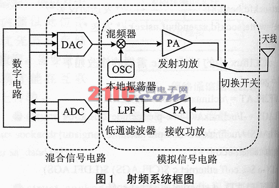
Generally, the functional block diagram of the RF chip is shown in the graphics card. With the development of wireless technology, the integration and performance of wireless transceiver chips are greatly provided, and the performance of the chip also has its own characteristics. Therefore, the choice of wireless transceiver chip is crucial in the design. The right choice can reduce the development difficulty, shorten the development cycle, reduce costs, and bring products to market faster. At present, the manufacturers of such chips mainly include Nordic, XEMICS, Chipcon, TI, and Maxim. When choosing a wireless transceiver chip, the following factors should be considered: power consumption, transmit power, receiving sensitivity, transmission speed, wake-up time from standby mode to working mode, the number of peripheral components required by the transceiver chip, chip cost, etc .; Pay attention to local radio regulations.
(3) Selection of discrete components
All RF chip manufacturers are trying to improve the integration of the chip, but there are still some components that are difficult or impossible to integrate into the chip. These discrete components are often placed outside the chip, such as crystal oscillator, PLL loop filter, VCO inductance, etc. In radio frequency circuits, the wavelength of electromagnetic waves can be compared with the size of discrete components. The Kirchhoff-type current and voltage laws commonly used in DC and low-frequency lumped parameter systems are no longer applicable. These discrete components must be considered High frequency characteristics and their distribution parameters. Therefore, when designing in detail, you should refer to the data sheet of the selected chip and related components.
2 System schematic design
The key to the hardware of the embedded short-range wireless communication system is its radio frequency circuit. Here, Maxim's MAX1472 and MAX1473 chips are used for RF circuit design. Figure 2 is the transmitter radio frequency circuit, and Figure 3 is the receiver radio frequency circuit.
MAX1472 is a miniature 3mm & TImes; 3mm pin SOT-23 package VHF / UHF based phase-locked loop ASK transmitter. When the operating voltage drops to 2.1V, the disconnected lithium battery works and only consumes 100nA in standby mode. During the transmission process, the transmission power of MAX1472 is -10dBm ~ + 10dBm. Working voltage 3.3V; when the transmitting power is + 10dbm, the working current is only 9.1mA. The highest data rate is 100kbps.
The MAX1473 is a 300-450MHz, 28-pin, superheterodyne ASK receiver in a SSOP package; it has a high sensitivity of -114dBm, and users above 50dB can choose center frequency image rejection and a 3.3V or 5V power supply operating voltage . In shutdown mode, the current is less than 1.5mA, and the current is 5.2mA when receiving; the data rate reaches 100kbps; the transition time from shutdown mode to effective data output is less than 250μs.
The MAX1473 includes a first-level automatic gain control (AGC) circuit that reduces the gain of the low crying amplifier (LNA) by 35dB when the RF input signal power is greater than -57dBm. The receiver uses a 10.7MHz intermediate frequency filter with received signal strength indication (RSSI), built-in on-chip integrated phase-locked loop and VCO, baseband data recovery circuit.
In the design of the schematic diagram, in order to improve the sensitivity of the system, special attention should be paid to the adaptation of the antenna, low crying amplifier (LNA) and crystal oscillator, as shown in Figure 3 marked three places 1, 2, and 3. 
3 PCB board design
High-frequency signals are prone to interference due to radiation, leading to ringing, reflexion crosstalk, etc .; and RF circuits are particularly sensitive to this, so attention must be paid to PCB board design. For this power supply design, a multi-layer board should be used under conditions permitting to provide a dedicated power layer and ground layer. If the power bus mode is adopted, the power line and the ground line should be thickened as much as possible; the through holes on the board (including the pins of the plug-in components, vias, etc.) should be reduced as much as possible; add more ground lines; separate the analog power supply and the digital power supply ; Isolate sensitive components; power lines can be placed on the side of the signal line to minimize the signal loop area and reduce the number of loops. Transmission interconnection should try to meet the following rules: Avoid transmission line impedance discontinuity (impedance discontinuity is the first point of transmission mutation, such as straight corners, vias, etc., it will generate signal reflection. For this reason, avoid routing Straight corners, 45 ° angle or arc routing can be used, as few holes as possible); do not use pile lines. Second, reduce crosstalk. Crosstalk is a coupling between signals. There are two types of capacitive crosstalk and inductive crosstalk. Generally, inductive crosstalk is much larger than capacitive crosstalk. Crosstalk can be suppressed by some simple methods: ①Because the magnitude of capacitive crosstalk and inductive crosstalk increases with the increase of load impedance, the interference sensitive signals caused by crosstalk should be properly terminated. ② Increase the distance between signal lines to reduce capacitive crosstalk. ③In order to reduce capacitive crosstalk, a ground wire can be inserted between adjacent signal lines; but it should be noted that this ground wire should be connected to the wire layer every 1/4 wavelength. ④ For inductive crosstalk, the loop area should be minimized, and if allowed, the secondary loop should be eliminated. ⑤ Avoid signal sharing circuit. Finally, as circuit speeds increase, electromagnetic interference (EMI) becomes more severe, and EMI must also be reduced. Ways to reduce EMI are usually: shielding, filtering, eliminating current loops and reducing device speed as much as possible. There are usually three options for filtering: decoupling capacitors, EMI filters, and magnetic components. The most common is decoupling capacitors, which are used for power line filtering. A 1μF ~ 10μF decoupling capacitor is usually placed at the power access circuit board to filter out low-frequency noise; a 0.01μF ~ 0.1μF decoupling capacitor is placed at the power supply pin of each source device on the board to filter out High frequency noise. Pay attention to the placement of decoupling capacitors.
4 RF chip and MCU interface
Realize data transmission through RF chip. There are usually three ways for the receiving MCU to collect the RF chip output signal: over sampling, pulse edge detection (edge ​​detecTIon), and using the MCU's universal serial communication port (UART).
When re-sampling, the output signal of the RF chip is re-sampled at a rate three times the bit rate, and a sampling weighting table is used. For noise suppression, it is suitable for occasions with long distance and high reliability requirements; however, the timing requirements are strict and the software implementation is more complicated. The interface between the RF chip and the MCU can use the input and output ports of the MCU.
The pulse edge detection uses digital signal pulses to achieve synchronization, and the RF chip output signal is used as the interrupt request signal of the MCU. The interrupt program calculates the sampling time of each bit and can process data streams of various rates; but each bit is sampled only once, which is more sensitive to noise, and the implementation algorithm is more complicated than repeated sampling. The interface between the RF chip and the MCU can use the interrupt system and input and output ports of the MCU.
To simplify the design, the universal serial communication interface (UART) of the MCU can be used. UART is more sensitive to noise, but it can be solved in software design, so this interface is usually used.
5 System transmission distance
(1) Wireless communication distance calculation
Here is the calculation method of wireless communication distance in free space propagation. The so-called free space propagation refers to the propagation of radio waves when the antenna is in an infinite vacuum, which is the ideal propagation condition. When a radio wave propagates in free space, its energy is neither absorbed by obstacles nor reflected or scattered. The communication distance is related to the transmitting power, receiving sensitivity and working frequency.
Loss of radio wave propagation in free space:
Los = 32.44 + 20lgd + 20lgf
Los-propagation loss, in dB; d-distance, in km; f-operating frequency, in MHz.
For example, a system with an operating frequency of 433.92 MHz, a transmit power of +10 dBm (10 mW), and a receiving sensitivity of -105 dBm travels in free space: â‘ By transmitting power +10 dBm, the receiving sensitivity is -105 dBm, and Los = 115 dB â‘¡D = 31km is calculated from Los and f.
This is the transmission distance under ideal conditions, and it will be lower than this value in practical applications. This is because wireless communication is affected by various external factors, such as the loss caused by the atmosphere, barriers, and multipath. Calculate the approximate communication distance by taking the above loss reference value into the above formula. Assuming that the loss caused by the atmosphere and occlusion is 25dB, the communication distance can be calculated as: d = 1.7km.
image 3
(2) Increase the wireless communication distance
When the operating frequency is fixed, the main factors that affect the communication distance are: transmit power, receive / transmit antenna gain, propagation loss, receiver sensitivity, etc. For the designer, some factors cannot be selected and changed, such as propagation loss, multipath loss, path loss, ambient absorption, etc .; and some factors can be controlled by the designer, such as transmit power, receive / transmit Antenna gain, receiver sensitivity, etc. By adjusting these factors, the transmission distance of the wireless communication system can be increased. To increase the transmission distance, designers often think of increasing the transmission power. But increasing the transmit power will bring some disadvantages. For example: due to the low conversion efficiency of the power amplifier, increasing the transmission power will greatly increase the power consumption of the system, which is very unfavorable for embedded systems; increasing the transmission power will produce greater harmonic interference and noise, and Communication channels have other effects, sometimes affecting the communication distance. Therefore, it is not recommended to increase the transmission distance to increase the transmission distance in embedded systems. A better way to increase the transmission distance is to increase the gain of the receiving / transmitting antenna by generally selecting a high-gain antenna. The use of high-gain antennas has the advantages of integrated antennas, small size, low cost, simple implementation, and no additional power consumption and components.
Conclusion
For a complete wireless system, there are antenna design, MCU and peripheral circuit design. In addition, because the reliability and bit error rate (BER, Bit Error Rate) of the RF link are several orders of magnitude higher than that of the conventional wired system, therefore, the embedded short-range wireless communication system must strengthen system testing, especially the system bit error Rate (BER) test. It is necessary to find out the background crying points in favor of excessive error codes and improve the performance of the system. Due to space limitations, this article does not stay overnight.
Piezo Siren,Piezo Siren 12V,120Db Piezo Siren,Loudest Piezo Siren
NINGBO SANCO ELECTRONICS CO., LTD. , https://www.sancobuzzer.com