| Abstract: DS8007 is a low-cost multi-protocol dual smart card interface that meets all the requirements of ISO 7816, EMV ™ and GSM11-11. This mixed-signal peripheral can manage all interface details between the microcontroller and two independent smart cards. This application note introduces some basic knowledge of smart cards and how to communicate with smart cards. It also provides software for smart cards to interface with DS5002 security processors via DS8007. What is a smart card? Smart cards are usually defined as small cards containing embedded integrated circuits. Due to embedded integrated circuits, smart cards are sometimes referred to as integrated circuit cards, or ICCs. Figure 1 shows a typical example. Because they can be applied to many different occasions, these cards replace the familiar payment cards (debit cards or credit cards), and they use magnetic stripes to store card account information. In the payment application, the transfer (relocation) to the smart card is mainly because it can increase the function, especially after using this technology can improve the security. However, the higher cost of smart cards must be considered when evaluating the last capability. 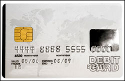 Figure 1. Examples of smart cards The integrated circuit embedded in the smart card can be a simple, non-volatile storage device, or some advanced circuits like a microcontroller, which can perform complex operations. A simple non-volatile storage device in the payment card can replace the magnetic stripe to store data. In many similar devices, some additional logic is combined in the memory bank to limit the reading of part or all of the memory bank. However, the true capability of smart cards is that the embedded microcontroller has the function of performing data operations and / or encryption. This processing power can improve safety performance. However, as the complexity increases, the cost of the card also increases. The cost of a smart card embedded in the Controller is between $ 7.00 and $ 15.00 (USD), while the cost of a payment card using a magnetic strip can be as low as $ 0.75¹ (USD). The higher cost of smart cards has slowed the overall shift from simple technology, but as the demand for security increases, so will the demand for smart cards. DS8007 provides all the electrical signals necessary when the microcontroller is physically connected to two independent smart cards. The device contains a dedicated internal timing circuit to control the automatic activation and deactivation of the card, and an ISO UART for data communication. The device can work at a power supply voltage of 2.7V to 6.0V. Through the charge pump and voltage regulator, it can also output two independent smart card supply voltages, each of which can be selected from 1.8V, 3.0V or 5V. Can communicate with the microcontroller through a standard parallel 8bit data line, can be configured for non-multiplexed mode, or data and address multiplexing. Smart Card Details The shape of most smart cards that people are familiar with is the size of a credit card. The phrase "smart card" can also be used to refer to a subscriber identification module (SIM). It is roughly the size of a postage stamp and is often used in cellular phones. This SIM shape can also be used in payment terminals to provide specific payment system data and detailed application information for the terminal. Credit card-sized devices (parts) are usually made of polyvinyl chloride (PVC), and generally have the account number molded and possibly an expiration date. Regardless of the form used, all electromechanical structural specifications are based on the ISO 7861 series of standards. In addition, a consortium of EuroCard®, MasterCard® and Visa® (EMV) companies has also developed a set of standards (called EMV specifications) specifically for solving smart cards and their application in payment systems. EMV specifications are usually based on ISO 7816 documents. Smart card contacts The above standards clearly define the number, rank, and function of smart card contacts. Figure 2 shows the location of the integrated circuit on the smart card and the size of the contacts. ISO 7816 defines 8 possible contact positions. Of these 8 positions, 5 are currently used in EMV applications. Table 1 lists the names and functions of these contacts. ISO 7816 defines contact C6 as VPP, but according to the EMV specification, the current card does not use this programming voltage. Contacts C4 and C8 are not used, and physical connectors are not required. Below is a more detailed discussion of each contact defined by the EMV specification. Table 1. Smart card connections
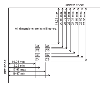 Figure 2. Contact size and location VCC contact (C1) This contact provides the supply voltage for the card. In the original specification, VCC included only 5V DC ± 10%. However, there is currently a phased transition to low voltage cards. Cards that can only support the original specifications are called Class A cards, and they will be replaced by Class AB or ABC cards by the end of June 2009. VCC specifications for different types of cards: Class A card: 4.5V ≤ VCC ≤ 5.5V @ ≤ 50mA Class AB: 2.70V ≤ VCC ≤ 3.3V @ ≤ 50mA Class ABC: 1.62V ≤ VCC ≤ 1.98V @ ≤ 30mA The DS8007 card interface includes a charge pump and a voltage regulator. When the device operates at a power supply voltage of 2.6V to 6.0V, it can provide the appropriate voltage for all three card types. I / O contact (C7) The I / O contacts on the smart card are used as input when receiving data from the terminal (receiving mode) or as output when sending data to the terminal (transmitting mode). In the receiving mode, the card recognizes valid data when the input meets the following specifications. Type A card input high voltage: 0.7 × VCC ≤ VIH ≤ VCC Input low voltage: 0.0 ≤ VIL ≤ 0.8V Rise time / fall time: ≤ 1µs AB or ABC type card input high voltage: 0.7 × VCC ≤ VIH ≤ VCC ≤VCC Input low voltage: 0.0 ≤ VIL ≤ 0.2 × VCC Rise time / fall time: ≤ 1µs In transmit mode, the I / O contacts will provide the following signal levels: Class A card output high voltage: 0.7 × VCC ≤ VOH ≤ VCC, -20µA <IOH <0, VCC = min Low output voltage: 0.0 ≤ VOL ≤ 0.4V, 0 <IOL <1mA, VCC = min Rise time / fall time: ≤ 1.0µs AB or ABC card output high voltage: 0.7 × VCC ≤ VOH ≤ VCC, -20µA <IOH <0, VCC = min Low output voltage: 0.0 ≤ VOL ≤ 0.15 × VCC, 0 <IOL <1mA, VCC = min Rise time / fall time: ≤ 1.0µs The EMV specification requires that the smart card's I / O contact driver should be in receive mode unless the I / O contact is sending data. Clock contact (C3) The clock contact is an input terminal, and the input source is an interface terminal, such as DS8007. This signal is used to control the data transmission clock during the transaction. The specified frequency range is 1.0MHz to 5.0MHz. This contact has the following electrical specifications: Class A card input high voltage: VCC-0.7 ≤ VIH ≤ VCC Input low voltage: 0.0 ≤ VIL ≤ 0.5V Rise time / fall time: ≤ 9% of clock period AB or ABC type card input high voltage: 0.7 × VCC ≤ VIH ≤ VCC Input low voltage: 0.0 ≤ VIL ≤ 0.2 × VCC Rise time / fall time: ≤ 9% of clock cycle RST contact (C2) The RST contact is the input terminal on the card, and the input source is the interface terminal. This signal is active low and will cause an asynchronous reset of the card. This contact has the same electrical characteristics as the CLK contact, but its maximum rise and fall times are 1.0µs. As can be seen from the above specification, the terminal that interfaces with the smart card must provide different power supply voltages and signal levels. The interface specification also requires that the terminal can withstand a short circuit between any two points of the card contact. For these reasons, the use of specialized equipment to provide the necessary power supply voltage and signal level is clearly more advantageous than using a large number of discrete analog ICs to build circuits. DS8007 is such a dedicated device. In addition to including analog circuits to implement these functions, it also contains FIFO and other numerical control logic, which can realize the state sequencing and synchronization required for a complete card operation. The terminal interface requires that the card's operation process includes the following steps: Insert the card into the terminal, connect the contacts and activate the card reset, establish communication between the terminal and the card (ATR timing-as follows) Perform the transaction to close the contact, remove the card and insert the card After completing the initial reset, the card will respond with a series of characters, called a response reset, or ATR. This series of characters will establish the initial communication details, including specific protocols, bit synchronization, and data transmission details required for subsequent communication. Since subsequent data transmission can change certain communication parameters, ATR only establishes the initial communication conditions. ATR will be described in detail in the following section. The meaning information of each character is serially communicated between the interface of the smart card and the terminal through bidirectional I / O contacts. The duration of a bit is defined as the basic unit of time, or ETU. The ETU time period has a direct linear relationship with the clock signal provided by the terminal through the CLK contact. The bit synchronization of characters during ATR is called the initial ETU. This initial ETU is defined by the following formula:
Where Æ’ is the frequency of the clock signal in hertz. After ATR, the bit duration is called the current ETU, which is a function of parameters F, D, and clock frequency (parameters F and D are discussed in more detail in the TA1 character section below)
Where Æ’ is the frequency of the clock signal in hertz. Each character in any communication consists of 10 bits, so the total duration is 10 ETUs. The first bit of the character is called the start bit, which is always low. Before the start bit, the I / O line will keep the default high level. The last bit of the character is the parity bit, which is either high or low, determined by the data source, so the total number of 1s in the character can be kept even. Figure 3 shows a legend for this bit pattern. 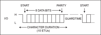 Figure 3. 10-bit character frame Smart card communication protocol In the ISO 7816 specification, four bits are used to select the communication protocol during card operation. Currently, 2 of the 16 available protocols are mainly used, and they are defined as T = 0 and T = 1. Both protocols are half-duplex (one-way each time) asynchronous communication. The T = 0 protocol is a character-based format, and T = 1 is a block-based format. All smart cards compatible with EVM must support the T = 0 or T = 1 protocol, and the terminal must support both methods. After the card is inserted into the terminal, and when all contacts remain in the "low" state, the power supply voltage is quickly applied to the VCC contacts. When the terminal determines that the voltage is stable and within the specified range, the terminal's I / O contact driver is set to receive mode, and its clock signal is transmitted to the CLK contact of the card. During the 200 cycles of clock signal initialization, the terminal's I / O line has been in the receiving mode, and the card will put its I / O line into the transmitting mode. After 40,000 to 45,000 clock cycles, the terminal releases a high active signal to the card's RST contact. After 400 to 40,000 clock cycles, the card responds with a series of character strings, called ATR. The information contained in the ATR will determine in detail how subsequent communications are implemented, including the choice of T = 0 or T = 1 protocol. If no protocol is specified, T = 0 is assumed. (There will be complete details of the ATR and the information contained in the ATR below.) Response reset (ATR) After being initially reset by the terminal, the EMV smart card responds with a string of characters called response reset or ATR. These characters include an initial character, TS, followed by up to 32 additional characters. Together, these characters provide the terminal with information on how to communicate with the card for subsequent work. The following section describes each character. The EMV specification defines the ATR content defined by protocol T = 0 as shown in Table 2, and when protocol T = 1 as shown in Table 3. Table 2. Basic EMV ATR (T = 0)
Table 3. Basic EMV ATR (T = 1)
TS initial character The first character of the ATR sequence is defined as the initial character TS. According to its bit pattern, this character synchronization information defines the polarity of all subsequent characters. The first four bits of TS are composed as follows: a low-level start bit, then two high-level bits, followed by a low-level bit. This fixed bit pattern ensures synchronization. The following three bits may all be high level to represent direct appointment, or all low level to represent reverse appointment. For direct agreement, the high level on the I / O line represents logic 1, and the least significant bit is sent first during data transmission. For the reverse convention, the low level on the I / O line represents logic 1, and the most significant bit is sent first during data transmission. Since the specification allows reverse conventions, EMV recommends that all current card designs use direct conventions. The last three bits are two high levels and one low level. The last bit in the ATR or any other 10-bit character frame is a parity bit. It will set high or low to ensure that the total number of 1s in the frame is an even number. T0 format characters The second character of the ATR sequence is defined as the format character, called T0. This character contains two parts, which are used to determine which characters will be included in the rest of the ATR sequence. The four most significant bits are represented by Y1, they represent whether TA1, TB1, TC1 or TD1 will be sent. For each logical 1 of Y1, the occurrence of each character is determined in the following way: Bit 8 (msb) = 1 means the character TD1 will be sent Bit 7 = 1 means the character TC1 will be sent Bit 6 = 1 means the character TB1 will be sent Bit 5 = 1 means the character TA1 will be sent The four least significant bits of T0 are represented by K. These bits will determine the number of "historical bytes" included in the remaining ATR series, 0 to 15. The history byte will convey some general information of the card, such as the manufacturer of the card, the chip in the card, the mask ROM in the chip, or the service life of the card. Neither the ISO 7816 nor the EMV specifications define exactly what (if any) information should be transmitted. We can see from Table 2 above that b7 and b6 of Y1 are high, and bits b8 and b5 are low ('6x'). This means that TC1 and TB1 will be sent, while the characters TA1 and TD1 will not be sent (as shown in the table). For protocol T = 0, characters TB1 and TC1 complete the most basic ATR sequence. In Table 3, bit 8 of Y1 is also high, so for protocol T = 1, the character TD1 will also be sent. Whether the TA1 character is T = 0 or T = 1, the basic EMV ATR response does not send the character TA1, which is defined in the ISO 7816 specification for other communications. When in use, TA1 will be divided into upper and lower nibbles. The upper nibble determines the clock rate conversion factor F, which is used to adjust the frequency of the clock signal. The lower nibble determines the bit rate adjustment factor D, which is used to adjust the subsequent bit duration of the ATR. These parameters are used in Equation 2 above. During the ATR, the initial ETU selects the default value, F = 372, D = 1. If it is not modified beyond the basic ATR, the default value will still be used in subsequent interactions. TB1 character The TB1 character conveys information about the smart card programming voltage requirements. Bits b1 to b5 (called PI1) carry the programming voltage, and bits b6 and b7 (called II) carry the maximum programming current required by the smart card. For the basic ATR, TB1 = '00' means that the VPP pin is not connected on the smart card. TC1 character The size of the TC1 character transfer N, which is used to determine the extra protection time to be added when the terminal sends consecutive characters to the smart card. This value has nothing to do with the characters sent by the card to the terminal or the two characters in the opposite direction. N is a binary number, which represents the ETU added as an extra guard time. When TC1 = 'FF', the minimum delay should be used between two characters. For protocol T = 0, this value is 12 ETUs, and for protocol T = 0, this value is 11. The size of N can be any value between 0 and 255. If TC1 does not return in ATR, the terminal will receive 00 by default and continue to work. Because this value can increase the time between character transmissions, it should be reduced in order to speed up transactions. TD1 character The TD1 character indicates which protocol will be used if more interface bytes are to be sent. The character TD1 is a specific example of the general character TDx. The most significant nibble of TDx represents whether TA (x + 1), TB (x + 1), TC (x + 1) or TD (x + 1) is to be transmitted. For each logic 1, whether each character sent subsequently appears is determined according to the following principles: Bit 8 (msb) = 1 means the character TD (x + 1) will be sent Bit 7 = 1 means the character TC (x + 1) will be sent Bit 6 = 1 means the character TB (x + 1) will be sent Bit 5 = 1 means the character TA (x + 1) will be sent The value of the least significant nibble of the TD1 character (unified as TDx) is either 0x0 or 0x1, respectively representing the protocol T = 0 or T = 1. If the protocol T = 0 is used, the character TD1 will not be included in the ATR sequence, and subsequent transmission will use the protocol T = 0. If the protocol T = 1 is used, the character TD1 will be included and its value will be 0x81. This value means that there will be TD2, and all subsequent transmissions will use the protocol T = 1. The TA2 character is not sent in the basic EMV ATR response regardless of the protocol T = 0 or T = 1, so it is defined by the ISO 7816 specification. The presence or absence of TA2 is used to determine whether the smart card works in special mode or transaction mode after ATR. Without TA2, the operation mode will be adopted. The TB2 character is not sent in the basic EMV ATR response regardless of the protocol T = 0 or T = 1, so it is defined by the ISO 7816 specification. The character TB2 transmits PI2, which determines the programming voltage value required by the smart card. When the character TB2 is present, the PI1 value in the character TB1 will be replaced. The TC2 character is not sent in the basic EMV ATR response regardless of the protocol T = 0 or T = 1, so it is defined by the ISO 7816 specification. When TC2 is present, it will specify the protocol type T = 0. TC2 will transmit the work waiting time integer (WI), which is used to determine the maximum interval between any character sent by the smart card and the previous character sent by the smart card or terminal at the rising edge of the start bit. The value of the work waiting time is calculated as follows:
Where D is the bit rate adjustment factor (see the introduction in section TA1 above). When TC2 is not included in the ATR series, WI = 0x0A is assumed as its default value. TD2 character The TD2 character has the same function as the TD1 character. See the TD1 introduction above for details. For protocol T = 1, TD2 appears in Table 3, and its value is 0x31. This value represents: there will be TA3 and TB3, no TC3 and TD3, and the protocol type will be T = 1. TA3 character The TA3 character is the integer size (IFSI) of the information field transmitted by the smart card. IFSI determines the size of the information field for the smart card. It is the maximum length of the information field (INF) portion of the data block that the card can receive. The size of the field can be any value between 0x01 and 0xFE. The values ​​0x0 and 0xFF are reserved for future use. In the basic ATR using the T = 1 protocol, the value range of TA3 is 0x10 to 0xFE, so it represents IFSC between 16 and 254 bytes. For ATR without TA3, the terminal will assume the default value of 0x20. TB3 character The TB3 character represents the value of the character waiting time integer (CWI) and block waiting time integer (BWI), which are used to calculate the character waiting time (CWT) and block waiting time (BWT). The least significant nibble (b1 to b4) of TB3 represents the value of CWI and the most significant nibble (b5 to b8) represents the value of BWI. In the basic ATR using the T = 1 protocol, the least significant nibble range of the TB3 character is 0 to 5 (CWI = 0 to 5), and the most significant nibble range is 0 to 4 (BWI = 0 to 4). The TC3 character is not sent in the basic EMV ATR response regardless of the protocol T = 0 or T = 1, so it is defined by the ISO 7816 specification. When TC3 is present, it represents the type of block error detection to be used. When there is no TC3, the default longitudinal redundancy check (LRC) will be used for block error detection. TCK character The TCK character is a check character, and its value can be used to check the integrity of the data sent during the ATR. As long as all the bytes between T0 and TCK are XORed, the result can be any value. TCK is not used when T = 0, but will return in ATR in all other cases. ATR Summary After the terminal receives the last character of the ATR sequence, all necessary parameters are sent from the card to the terminal, and the necessary adjustments to the interface parameters of the DS8007 can be made. This allows the subsequent communication to start. Application Protocol Data Unit (APDU) As mentioned earlier, the next stage of card operation is the execution of a transaction. The specific operations performed during the transaction depend on the type of card, account (credit card, debit card, etc.) and the user's request. No matter what specific operation, the transaction is completed by the terminal sending commands to the smart card. The smart card performs the requested service and may reply with a result. The operation of the card can be as simple as reading a location in the memory, or as complex as performing encryption. Regardless of the operation, the communication between the terminal and the card is achieved through the application of protocol data units, or APDUs. When executing an application, the smart card and the terminal must exchange information. The sharing of information is done through command and response data exchange. The terminal creates and sends a command to the smart card, and then the smart card decodes the command and sends a response. This command response message pair is called an application protocol data unit (APDU). The specific command information (C-APDU) sent by the terminal will receive the specific response information (R-APDU) from the card. These messages are called APDU command response pairs. The format of these two types of information is detailed in the EMV specification. Their format is as follows. The C-APDU format terminal initiates all command APDUs. They must contain a 4-byte header, followed by an optional data section, whose length is variable. The number of bytes of data in the C-APDU is specified by the command byte Lc, and the number of bytes the terminal wishes to receive from the smart card response is specified by the instruction Le. Table 4 shows the format of the C-APDU, and Table 5 shows the character description. Table 4. APDU command structure
Table 5. APDU command content description
The first byte of the command APDU is defined as the command category, called CLA. This byte can be any 8-bit value except 0xFF, but currently only 0 to 8 are used in the highest priority nibble. When the highest priority nibble is 0, it is defined as an inter-industry command, and when it is 8, it is defined as dedicated to the EMV specification. The second byte of the command APDU is the instruction code, called INS. This byte is only valid if the least significant bit is 0 and the most significant nibble is not 6 or 9. In the necessary header, P1 and P2 contain the parameters of a specific command, which can be any value. If not used, the parameter byte must take the value 0x00. R-APDU The smart card will return a response after receiving and decoding the APDU command from the terminal. As defined in the specification, the response consists of a variable-length optional data part followed by a required two-byte trailer. Table 6 shows its format, and Table 7 shows the content of the APDU response. Table 6. APDU card response format
Table 7. APDU command response content
The expected length of the smart card response is sent through the Le code portion of the APDU command. The actual length of the response is called Lr. Although the card does not send the value of Lr, the terminal can calculate this value if required by the application. For the end of the normal command, the smart card will return 0x90 in SW1 and 0x00 in SW2. Any other response indicates that an error or alarm has occurred². Sample code The software provided in this application note is included in the downloadable file an4029_sw.zip. This file includes all the C (main.c, ds8007.c, LCD_Funct.c) and assembly language (Startup.a51) source code needed to generate an executable hex file (ds8007.hex). The code is compiled and linked by Keil PK51 Professional Development Kit and µVision® Integrated Development Environment (IDE). The µVision project file (ds8007.Uv2) is also included in the .zip file. Maxim provides .HEX files that can be loaded and run on the DS8007 smart card interface board, which is included in the DS8007 evaluation (EV) kit. The sample software implements a complete smart card working process, including power-on, ATR, APDU, and power-off operations. When connected to a dumb terminal, the circuit board will generate an RS-232 serial output of 38,400 baud through software. This output is shown in Figure 4 below. The detailed description of the software is beyond the scope of this application note, but the source code we provide can be used as the basis for a complete set of smart card interfaces based on the DS5002 security processor and DS8007 multi-protocol dual smart card interface chip. 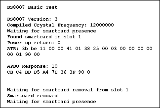 Figure 4. Software output We used Advanced Card Systems (ACS) 's microcontroller-based smart card to test this example software. As a microcontroller-based device, this card performs the functions in the embedded operating system called ACS Smart Card Operating System Version 1, or ACOS1. This card has the following characteristics: 8kB EEPROM storage area for application data compatible with ISO 7816-3, T = 0 protocol DES and MAC capabilities Session key based on random number PIN can be changed by the cardholder for mutual authentication The documentation of the key pair ACOS1 indicates that this card will respond to reset with 19 bytes of data. As can be seen from Figure 4, the return value for T0 is 0xBE. The high nibble 0xB means that the ATR will contain TA1, TB1 and TD1 in addition to TS. The low nibble 0xE means that there will be 14 historical bytes in the ATR response (see the description of the character T0 above). Therefore, the ATR from the card contains a total of 19 bytes. For this example software with an APDU, execute the start session command. This command has the following format:
The response to the start session command has the following format;
The software output shown in Figure 4 indicates that the returned random numbers from the card are 0xCB, 0xC4, 0xBD, 0xD5, 0xA4, 0x7E, 0x36 and 0x3F. It also indicates that the return status is 0x90, 0x00, which indicates that the command was successfully completed. Conclusion DS8007 is a mixed-signal peripheral that eases the interface between the microcontroller and the smart card and provides all the electrical signals necessary to physically connect two independent smart cards. The dedicated internal timing circuit is used to control the automatic activation and deactivation of the card, and there is also an ISO UART for data communication. DS8007 can work under the power supply voltage of 2.7V to 6.0V. Through the charge pump and voltage regulator, it can also output two independent smart card supply voltages at the same time, each of which can be selected from 1.8V, 3.0V or 5V. It can communicate with the microcontroller through a standard parallel 8-bit data line, and can be configured as a non-multiplexed method or a data and address multiplexed method. Through the DS5002 secure microprocessor and using DS8007 as its smart card interface, the software we provide implements a complete smart card session. The characters returned by the smart card in its ATR are output on the serial port of the board at a baud rate of 38400, and the card sends the "Start Session" command APDU. The resulting random number will also be output on the serial port. | |||||||||||||||||||||||||||||||||||||||||||||||||||||||||||||||||||||||||||||||||||||||||||||||||||||||||||||||||||||||||||||||||||||||||||||
Football Stadium Advertising LED Screen
This series is a classic football field advertising LED Screen, which is specially used for advertising display in various stadiums, such as football fields, basketball courts, badminton courts, tennis courts, volleyball courts and other competitive sports halls. Football Stadium Advertising LED Screen with IP65 waterproof level, excellent anti-collision ability, can resist the impact of balls. High brightnesee makes good perfomance even under sunshine. Good protection design on top of cabinet with thick anti-collision cotton.

Football Stadium Advertising Led Screen,Led Panel Display,Led Video Panel, Football Cup Led Display Billboards
Guangzhou Cheng Wen Photoelectric Technology Co., Ltd. , https://www.leddisplaycw.com