Multichannel pulse amplitude analyzers and ray energy spectrometers are commonly used in nuclear monitoring and technology applications. In the 1990s, a new multi-channel spectrometer based on high-speed nuclear pulse waveform sampling and digital filter forming technology was introduced abroad, which made digitalization an important direction for the development of pulse energy spectrometer. Domestic spectrometer technology has been stuck at the level of analog technology for many years, and digital energy spectrum measurement technology is still in the method research stage. In order to meet the growing demand for high performance spectrometers, there is an urgent need to develop a digital gamma spectrometer. The nuclear energy spectrum displayed on the display by a nuclear pulse analyzer helps people understand the extent of radioactivity from nuclear matter.
1 Advantages of digital multichannel analyzer
A large number of scholars in China use the nuclear spectrometer analog circuit to realize the processing of pulse accumulation. Since the whole process is realized by analog circuits, it has been plagued by various unfavorable factors: the limited processing capability of the analog filter shaping circuit does not meet the requirements of optimal filtering; the energy resolution of the analog system is significant at high count rates. Decline, low pulse pass rate; inherent temperature drift and difficult adjustment of the analog circuit, resulting in system stability, linearity and low adaptability to different applications; more complex applications such as pulse waveform recognition, charge trapping effect correction, etc. The occasional simulation system is not up to the task.
In comparison, the performance of the digital pulse amplitude analysis system is significantly better than the analog pulse analyzer. The digital analyzer has the following advantages: it realizes the stability and reliability of the system through software implementation; it can use the digital signal processing method to achieve optimal design for the input noise characteristics to achieve the best or quasi-optimal filtering effect; The anti-stacking ability is strong, and the pulse passing rate is higher under the same energy resolution; the parameters are controlled by the program, and the adjustment is convenient and simple.
2 overall design
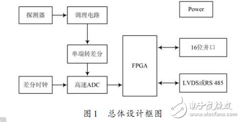
This scheme designs a hardware platform based on programmable gate array multi-channel pulse amplitude analyzer. Figure 1 is the overall design block diagram. The nuclear pulse signal output by the detector is simply conditioned by the front-end circuit. After single-ended to differential, the high-speed ADC with a sampling rate of 65 MHz is subjected to analog-to-digital conversion under the control of the FPGA to complete the core. The digitization of the pulse and the formation of a nuclear energy spectrum in the FPGA by the digital nuclear pulse processing algorithm can be transmitted to other spectral data processing terminals through a 16-bit parallel interface, or remotely transmitted through the LVDS/RS 485 interface. It is important to note that due to the high-speed AD pre-position, the conditioning circuit should meet the requirements of wideband, high speed, and dynamic adjustment of circuit parameters to adapt to the signals output by different types of detectors, so as to better utilize the advantages of digital technology.
3 specific hardware design
3.1 front end circuit
The front end circuit consists of a single-ended to differential and high speed ADC circuit. Differential circuits are widely used due to their good resistance to common mode interference. Since the pulse signal output from the conditioning circuit is a unipolar signal, if it is directly sent to the ADC, half of the dynamic range will be lost. In the design, an appropriate bias voltage is added to the op amp to convert the unipolar signal into a bipolar signal and then sent to the ADC to ensure the dynamic range. While converting the signal from single-ended to differential, anti-aliasing filtering is performed to complete the bandwidth adjustment.
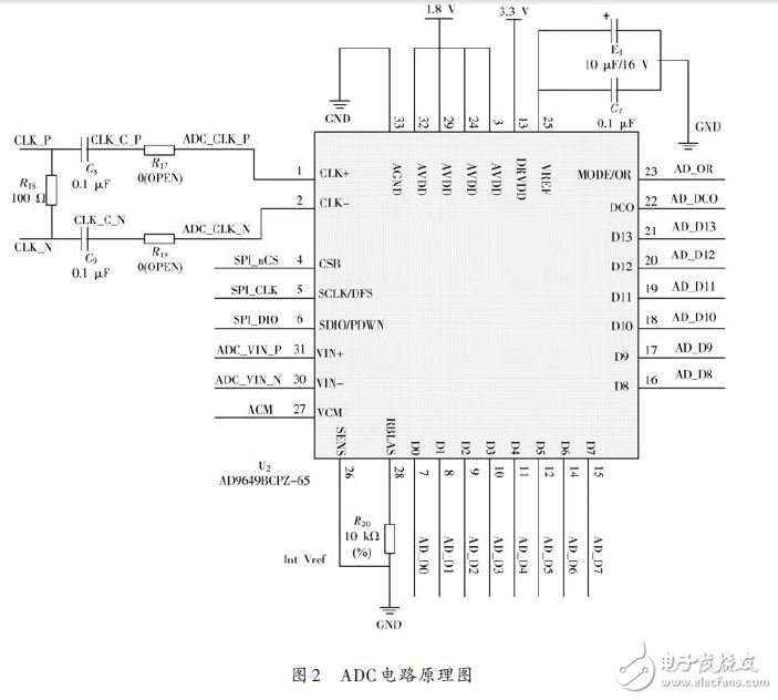
This design uses the AD9649-65 high-speed ADC to achieve analog-to-digital conversion of the core pulse. The AD9649 is a 14-bit parallel output high-speed analog-to-digital converter with low power consumption, small size, and good dynamic characteristics. When the signal passes through the conditioning circuit and passes through the differential circuit to the single-ended circuit, it enters the ADC as a differential signal. Under the control of the differential clock, it is converted into 14-bit data and enters the FPGA. The high-speed A/D is in the external FPGA. The signal is sampled under control. The sampled digital signal is then sent to the FPGA for amplitude extraction of the digital core pulse. Figure 2 shows the schematic of the A/D conversion. The AD9649 performs A/D conversion under the synchronization of the differential clock. D0~D13 are 14 valid output data bits.
Reset Lockout
Prevents reset if GFCI is damaged or failed to provide ground fault protection
Complies with NEC ® requirement, by blocking access to the contacts unless the plug is fully inserted
Only 1.22" Protrusion into Wallbox
Takes up to 20% less space in the wallbox vs. other GFCIs for easier installation
Multi-functional Status Indicator Light
Red and Green LED indications provide simple, intuitive feedback on power, voltage and protection status
Terminals Withstand
Tolerate high-torque;power tool installation;and prevents wire pullout
Tamper-Resistant Shutter mechanism
TR GFCI UL,New Version TR GFCI UL,TR Socket GFCI Outlets,New VGersion GFCI with TR Receptacle
Hoojet Electric Appliance Co.,Ltd , https://www.hoojetgfci.com