The LM4702 is designed for consumer applications where high sound quality is required and high power output is required. The output power of the amplifier can be adjusted according to changes in the supply voltage and the number of output devices. The audio amplifier designed with the LM4702 can output more than 300W per channel on an 8Ω load. LM4702 pdf datasheet
The LM4702 contains an overheat protection circuit that stops when the temperature exceeds 150 °C. In addition, the LM4702 has a mute function that, when enabled, attenuates the input drive signal and mutes the amplifier output.
First, the functional characteristics LM4702 has a total of three levels, in terms of application and performance levels span a large range. The LM4702C is designed for high-quality, high-power applications; the LM4702B (previously available) can be used with higher operating voltages; the LM4702A (in trial) is positioned for the highest-end applications with the highest operating voltage. All three levels have an ultra-wide operating voltage, with the LM4702A being ±20 to ±100V, the LM4702B being ±20 to ±100V, and the LM4702C being ±20 to ±75V. Its equivalent noise is 3uV, PSRR is 110dB, and THD is 0.001%. In addition, the LM4702 has some excellent features such as adjustable output power, fewer external components, external compensation, thermal protection and mute. They are widely used in car audio, AV home theater, Hi-Fi audio, stage audio and industrial control.
Figure 1 shows the appearance and pins of the LM4702. Figure 2 shows a typical application circuit for the LM4702. Figure 3 is its THD+N and output power diagram. 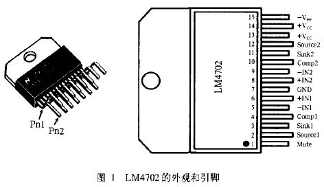
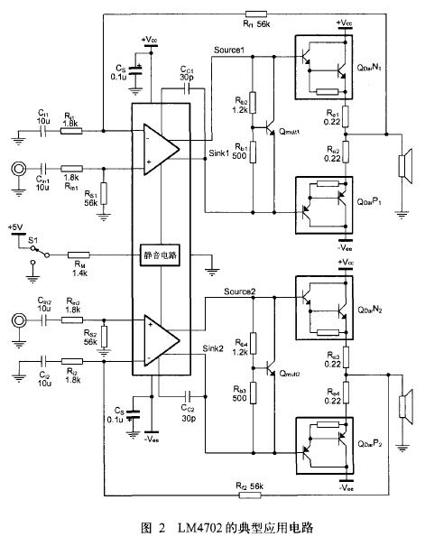
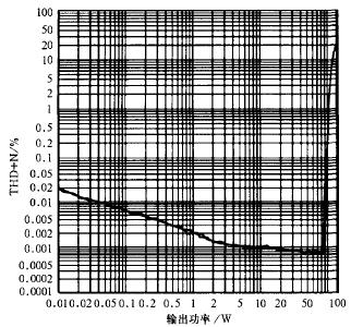
Figure 3 THD+N and output power diagram
(RL=8Ω, VSupply=±50VDc)
1. Mute function
The mute function of the LM4702 is controlled by the current flow into the mute pin. If the current flowing into the mute pin is less than 1 mA, the chip is muted. This can be done by shorting to ground or floating the mute pin. If the current flowing into the mute pin is 1 to 2 mA, the chip will be in playback mode. This can be done by connecting the power supply to the mute pin (Vmute) via a resistor (Rm). The current flowing into the mute pin can be calculated by the formula
Imute=(Vmute-2.9)/Rm to calculate. For example, if a 5V supply is connected to the mute pin through a 1.4kΩ resistor, the mute current will be .5mA, within the specified range. It is also possible to use Vcc to power the mute foot, at which point Rm needs to be recalculated accordingly. Currents flowing into the mute pin are currently not recommended to be greater than 2 mA because the LM4702 may be damaged.
It is highly recommended to switch this function quickly between mute and play mode by means of a toggle switch that is connected to the mute pin and to the ground or power supply via a resistor. Slowly increasing the mute current may cause DC voltage to be generated at the output of the LM4702, causing the horn to be damaged.
2. Thermal Protection The LM4702 has a complete thermal protection system to prevent the hot pressing of the system for a long time. When the internal temperature of the chip exceeds 150 °C, the LM4702 automatically turns off. When the temperature inside the chip drops to 145 °C, it starts working again. If the temperature continues to rise to 150 °C, the chip continues to turn off. Therefore, if a short-term failure occurs, the chip is allowed to heat up to a certain high temperature, but if it is a continuous failure, it may cause it to work under a thermal opening and closing condition of 145 ° C to 150 ° C. In this way, the thermal stress of the chip is greatly reduced by the cycle, thereby greatly improving the reliability under continuous failure conditions. Because the wafer temperature is directly related to the temperature of the heat sink, the heat sink must be selected to ensure that the overheat switch does not trigger under normal conditions. The best heat sinks allowed by cost and space ensure that any semiconductor device operates stably for long periods of time.
3. Power consumption and heat dissipation <br> In the playback mode, its operating current is constant regardless of the input signal amplitude. Therefore, the power consumption is constant for a given voltage and can be expressed by the formula PDMAX = Icc × (Vcc - Vee). A quick calculation for PDMAX is to multiply the entire voltage by a current of approximately 25 mA (the current will vary slightly over the operating range).
The choice of the heat sink of the high power amplifier is solely to maintain the temperature of the wafer at a certain level to ensure that the thermal protection system is not triggered at a certain level. The thermal resistance θJA (Junction to Ambient) between the wafer and the outside air is related to the environment. It consists of three thermal resistances, θJC (wafer to package), θCS (package to heat sink), and θSA (heat dissipation). Tablet to the environment). θJC is 0.8 ° C / W in the LM4702. After using a heat resistant alloy, θCS is approximately 0.2 °C/W. Because heat flow (power consumption) is similar to current flow, thermal resistance is like resistance, and temperature is reduced like voltage drop. The power consumption of the LM4702 can also be expressed as
PDMAX=(TJMAx-TAMB)/θJA
When TJMAx=150°C, TAMB is the ambient temperature of the system, and θJA=θJC +θCS+ θSA The maximum thermal resistance θSA of the heat sink is θSA=[(TJMAX-TAMB)-PDMA×(θJC+θCS)]/PDMAX
Again, the value of θSA is related to the system designer's requirements for the amplifier. If the ambient temperature of the amplifier is higher than 25 ° C, the thermal resistance of the heat sink needs to be smaller under other conditions.
4. Proper selection of external devices <br> In order to meet the design requirements of the application, the external device should be properly selected. Let's talk about the choice of peripheral device values ​​that will affect gain and low frequency response. The gain of each non-inverting amplifier is determined by resistors Rf and Ri, as shown in Figure 2. The gain of the amplifier can be expressed as
Av=1+Rf/Ri
For best signal to noise performance, lower resistance values ​​can be used. Ri usually takes 1kΩ and then determines the value of Rf based on the design magnification. For the LM4702, the amplification factor must be no less than 26dB, and if it is less than 26dB, it will be unstable. Ri and Ci in series (shown in Figure 2) form a high-pass filter, and the low-frequency response is determined by these two components. This -3dB frequency point can be obtained by
Fi=1/(2Ï€RiCi)
If an input coupling capacitor is used to block the DC from the input, a high-pass filter (combination of CIN and RIN) will be generated there. When using an input coupling capacitor, RIN must be used to set the DC bias point at the amplifier input. The -3dB frequency response generated by the combination of CIN and RIN can be expressed by
fIN=1/(2Ï€RINCIN)
When the input is left floating, a large change in the RIN value may be observed at the output. Decreasing the value of RIN or smoothing the input can make this change disappear. When the RIN is reduced, the CIN should be increased accordingly to ensure that the -3dB frequency response is unchanged.
5. Avoid thermal runaway when used as a bipolar output
When using the bipolar transistor as the output stage for the LM4702 (as shown in Figure 2), the designer must be aware of the problem of thermal runaway. Thermal runaway is due to the temperature dependence of Vbe (the intrinsic nature of the transistor). When the temperature rises, Vbe drops. In fact, the current flows through the bipolar transistor, heating the transistor, but lowering Vbe, which in turn increases the current strength and begins to cycle. If the system is not properly designed, this positive feedback mechanism will destroy the bipolar transistors in the output stage. The first recommended method is to use a heat sink on the bipolar output transistor to avoid thermal runaway, which will lower the temperature of the transistor.
The second recommended method is to use the emitter negative feedback resistor (Emitter Degeneration Resistor, Re1, Re2, Re3, Re4 in Figure 2). As the current increases, the voltage of the emitter's negative feedback resistor also increases, which reduces the voltage between the base and the emitter. This mechanism can help limit current and neutralize thermal runaway.
A third recommended method is to use a "Vbe multiplier" to clamp the bipolar output stage, as shown in Figure 2. This Vbe multiplier consists of a bipolar transistor (Qmult, as shown in Figure 2) and two resistors, one from the base to the collector (Rb2 and Rb4 in Figure 2) and the other from the base to the emitter. Pole (Rb1 and Rb3 in Figure 2). The voltage from the collector to the emitter (which is also the bias voltage of the output stage) Vbias = Vbe (1 + Rb2 / Rb1), which is why this cycle is called the Vbe multiplier. When the Vbe multiplier transistor Qmult is connected to the heat sink like a bipolar output transistor, its temperature will be synchronized with the temperature of the output transistor. Its Vbe is also temperature dependent, so when the output transistor heats it, it will draw more current. This will limit the current that the base enters the output transistor, thereby neutralizing thermal runaway.
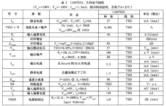
Table 1 shows the electrical characteristics of the LM4702 C operating voltages of ±75V and ±50V. Table 2 shows the electrical characteristics of the LM4702A and B when the operating voltage is ±100V.
Table 1 Electrical characteristics of the LM4702C
(Imute=1.5mA, TA=25°C unless otherwise stated) 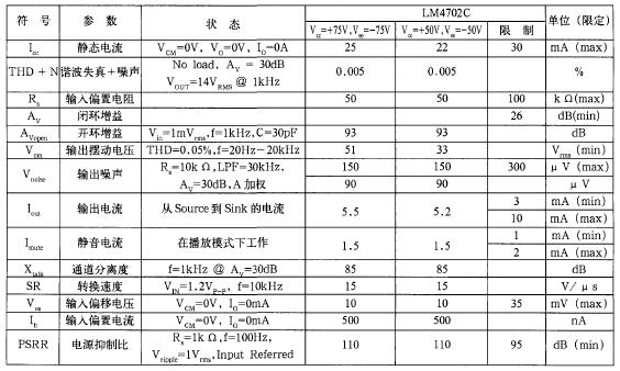
Note: 1. Typical values ​​are measured at 25 ° C, representing the standard of the parameters.
2. The scope of testing guarantees the average factory quality level of National Semiconductor.
3. The maximum/minimum specification range of the data is guaranteed by design, testing and statistical analysis.
This article refers to the address: http://
LED Tube Light is one of famous product in our company, high luminous and high efficiency. Wattage is optional. 4W, 6W, 8W, 10W, 17W, 22W and so on. LED Tube Light has quality assurance. All the products are inspected to meet with CE, RoHS standards, safe for user. Our long-term, strategic, stable partnerships with key component suppliers ensure our products quality and reliability. Goods must be 100% inspected OK by QC before shipping. We believe that the quality of our products and service will satisfy you.
Led Tubes,24W Led Tubes,20W Led Tubes,18W Led Tubes
SHENZHEN KEHEI LIGHTING TECHNOLOGY CO.LTD , http://www.keheiled.com