With the development of information technology, the bandwidth requirements of digital video signals for multimedia, virtual reality and network technologies are increasing, and the demand for data transmission has increased dramatically. Video image transmission technology with rich information has attracted much attention. Traditional video transmission methods have significant limitations in terms of speed, noise, EMI/EMC, power consumption, and cost. Therefore, the use of new I / O interface technology to solve the problem of video image transmission has become increasingly prominent. The low voltage differential signaling technology referred to as LVDS (Low Voltage Differential Signal) technology has the characteristics of high speed and low cost, which provides a possibility to solve the bottleneck problem of video transmission.
The core of LVDS technology is to transmit data with high-speed differential transmission with very low voltage swing, which can realize point-to-point or point-to-multipoint connection and long-distance signal transmission. It features low power consumption, low bit error rate, low crosstalk and low radiation. The transmission medium can be a copper PCB connection or a balanced cable. LVDS technology is a low-swing general-purpose I/0 standard. Its low-swing and low-current drive output achieves low noise and low power consumption, solves the bottleneck problem of physical layer point-to-point transmission, and meets the requirements of high-speed data transmission.
The LVDS technology is applied to the digital video transmission system, and the system can meet the requirements of real-time, stable and high-speed transmission of image data through reasonable scheme design.
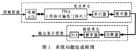
1 Digital video transmission system hardware design The digital video transmission system consists of a transmitting unit and a receiving unit. The functional block diagram is shown in Figure 1. The transmitting unit is mainly composed of an FPGA, an A/D converter, a serializer and a signal pre-emphasis buffer, and mainly performs digitization of the analog video signal and digital image information is serially driven and transmitted to the receiving unit. The receiving unit is mainly composed of an LVDS equalizer, a deserializer and a D/A, and mainly completes the deserialization of the serial differential signal, restores the parallel digital signal information, and converts the de-serialized signal into an analog video through D/A. signal.
This article refers to the address: http://
1.1 FPCA (Field Programmable Gate Array)
The solution uses the APAl50 from the second generation of Flash-based programmable device ProASIC Plus from Actel. This family of devices features ASIC (Application Specific Integrated Circuit) performance and FPGA flexibility, with 150 000 system gates. The logic unit is 6 144, with 36 Kb of dual-port SRAM and 2 phase-locked loop (PLL) cores. It supports 3.3 V, 32 bit, 50 MHz PCI bus, and the system has external performance of 150 MHz. Density, low power, non-volatile and repeatable programming. Because the ProASIC Plus family of FPGAs is based on the Fla-sh technology, the Flash switch is used to hold the internal logic, so no additional components are needed. Since there is no need for a power-on configuration process, it has the feature of working immediately after power-on. In addition, it is highly confidential, and the user can program a multi-bit key to prevent the outside world from reading or changing the configuration of the device. The APAl50 is mainly used to implement logic control, A/D sampling control, digital image enhancement and other functions.
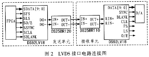
1.2 LVDS interface circuit design LVDS interface circuit consists of serial / deserializer, pre-emphasis and equalizer, is mainly responsible for the conversion and transmission of LVDS signals, is the key to the overall system design. 2 is a system LVDS interface circuit connection diagram, in which the serializer DS92LV18 converts the image data outputted by the FPGA and the clock and synchronization signals related to the image into a serial LVDS signal output, which is pre-emphasized by the DS25BR120 interface device and transmitted to The equalizer device DS25BR110 of the receiving unit, the equalized LVDS signal is restored to the parallel signal to the D/A converter for digital/analog conversion by the deserializer DS92LV18.
1.2.1 Serializer/Deserializer The serializer and deserializer use the 18-bit high-performance serial/deserializer DS92LV18. Its main performance features: clock frequency 15~66 MHz, can support 0.27~1. 188 Gb/s payload; transceiver design, built-in transmit/receive digital phase-locked loop, providing frame synchronization, frame detection, clock recovery; "plug and play" synchronous operation, no system required for live plugging Intervention. DS92LV18 mainly converts digital image data, clock and synchronization signals into parallel LVDS signals in the transmitting unit of the system. In the receiving unit, the serial LVDS signal data is mainly deserialized into parallel image data. Clock and sync signal. Figure 3 is a schematic diagram of the structure of the DS92LVl8.
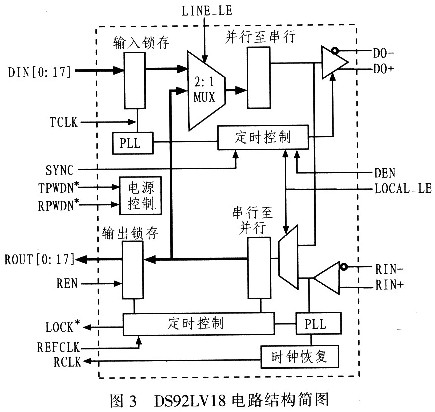
The pin configuration of the DS92LVl8 is as follows:
DIN[0:17]: 18-bit parallel LVTTL/LVCOMS input data signal;
TCLK: The encoding clock. When the encoder is working, the clock signal is encoded by the phase-locked loop 20 times and then encodes DIN[0:17] and TCLK into a 20-bit serial data signal, with LVDS standard level signals from D0+ and DO-output, the application requires the same frequency as the decoding clock REFCLK, and the deviation of the two clock frequencies cannot exceed 5%;
SYNC: Encoder operation control signal, set low when the encoder and decoder are working;
TPWDN, DEN: Encoder working control signal, set high level when the encoder is working; set low level when the decoder works;
RPWDN, REN: decoder work control signal, when the decoder works, set high level: when the encoder works, set low level;
RIN+, RIN-: decoder input serial LVDS signal;
ROUT[O:17]: 18-bit parallel LVTTL signal output by the decoder;
RCLK: decoder output clock, when the decoder works normally, the clock is at the same frequency as the input decoding clock REFCLK;
LOCK: decoder working state indication signal. When the decoder works abnormally, the signal is high level, and the error rate of the system transmission can be detected by detecting the signal;
LINE_LE, LOCAL_LE: feedback signal, can be used for device working state detection, set low in practical applications;
AVDD: analog power supply, 3.3V power supply; AGND: analog ground;
DVDD: digital power supply, 3.3V power supply; DGND: digital ground; PVDD: phase-locked loop power supply, 3.3V power supply; PGND: phase-locked ground.
1.2.2 Buffers and Equalizers Although the LVDS serializer/deserializer can drive the connection cable, the length of the cable is limited, typically no more than a few meters. Since the system requires long-distance transmission of data, in order to solve the design problem of long-distance transmission, pre-emphasis and equalization of high-speed serial digital signals in the transmitting unit and the receiving unit are considered. The pre-emphasis function not only compensates for the loss of high-frequency cables, but also enhances the data transfer capability of the cable and backplane, allowing the system to support longer distance transmissions. The function of the equalizer is to compensate for the channel loss and filter out the noise so that the serial digital signal from the cable can restore its original strength.
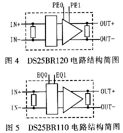
With the single-channel LVDS buffers DS25BRl20 and DS25BRll0, the signal integrity is guaranteed even at transmission speeds up to 3.125Gb/s. The structure diagrams of DS25BRl20 and DS25BR11O are shown in Figure 4 and Figure 5. The DS25BRl20 has a four-stage transmission pre-emphasis function. You can select different pre-emphasis levels by setting PE0 and PE1. The DS25BRll0 has four levels of receive equalization function. EQ0 and EQl select different equalization levels. Both devices have built-in 100Ω input and output termination matching resistors, so they can be directly connected to the serial/deserializer DS92LVl8 output and input terminals, eliminating the need for external matching resistors, reducing the number of peripheral devices and simplifying the PCB. wiring.
2 Digital video transmission system implementation In this system, the transmitted digital image resolution is 512x256x10 bit, and the encoding clock and decoding clock are both 40 MHz. In the design process, the transmitting unit and the receiving unit are 4-layer boards, which are divided into LVDS signal layer, ground layer, power supply layer and TTL signal layer from the top layer to the bottom layer, and are connected by shielded twisted pair cable. The LVDS signal is not only a differential signal but also a high-speed digital signal. Therefore, when performing PCB design with LVDS signals, it is very important to achieve impedance matching to prevent signals from being reflected at the transmission line terminals. Otherwise, the reflection caused by the mismatch of the differential impedance not only weakens the signal, but also increases the common mode noise, thereby generating electromagnetic radiation. Therefore, the wiring should pay attention to: 1) LVDS buffer DS25BRl20 and equalizer DS25BRllO should be as close as possible to the DS92LV18 output and input; 2) the length of the differential pair match each other, the distance between the two lines in the differential pair should be It may be short and the distance between the two differential lines should be as consistent as possible to avoid the discontinuity of the differential impedance: 3) The LVDS signal trace should be as short and straight as possible, and the arc or 45° fold line should be taken when turning. And try to reduce the vias. 4) Use a distributed number of capacitors to bypass the LVDS device with the surface mount capacitor placed as close as possible to the power/ground pins. For the DS92LVl8, if the PVDD (phase-locked loop power supply) is not isolated from AVDD and DVDD, use a π-type (CRC or CLC) filter next to each PVDD pin for filtering.
After the experiment, the digital video transmission system unpacked the data without error in the data transmission, and the synchronized signals such as the clock and the line field which are decomposed are compared with the original signal with a small phase delay, and the restored image is clear and undisturbed. Real-time transmission of video images is realized to meet engineering application requirements. If the image descrambled by the receiving board needs to be subjected to subsequent image processing, it is recommended to add an FPGA after the deserializer of the receiving board, and connect the deserialized parallel signal to the FPGA for processing on the timing, such as phase alignment, etc., the effect is will be better.
3 Conclusion With the sharp increase in the demand for high-resolution, long-distance digital video transmission, LVDS technology will have broad application prospects due to its high-speed transmission capability, low noise interference, strong integration capability, low cost, and low power consumption. . The LVDS-based video transmission system designed in this paper realizes real-time long-distance transmission of digital video. The scheme is versatile and scalable, and can be applied to video transmission systems with higher frame rate and resolution. Road video transmission system to meet the engineering application requirements of digital video transmission.
Coaxial Cable,Coax Cable,BNC Cable,CCTV Pre-made Cable,DC power splitter
Chinasky Electronics Co., Ltd. , https://www.chinacctvproducts.com