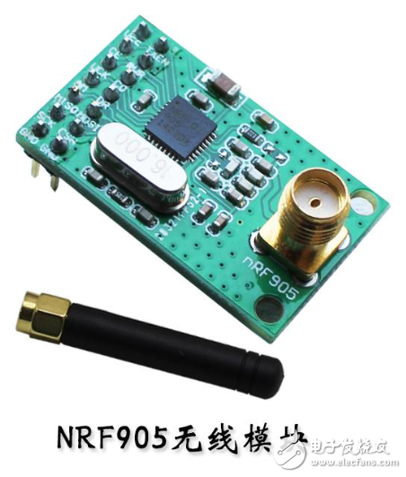
The nRF905 wireless chip is a sub-1GHz wireless data transmission chip produced by Norwegian NORDIC, which works mainly in the ISM bands of 433MHz, 868MHz and 915MHz. The chip has built-in frequency synthesizers, power amplifiers, crystal oscillators and modulators. The output power and communication channels can be configured through the program. Ideal for low power, low cost system designs.
The nRF905 uses Nordic's VLSI ShockBurst technology. ShockBurst technology enables the nRF905 to deliver high-speed data transfers without the need for expensive high-speed MCUs for data processing/clock coverage. By placing high-speed signal processing associated with the RF protocol into the chip, the nRF905 provides the application's microcontroller with an SPI interface at a rate determined by the interface speed set by the microcontroller itself. The nRF905 reduces the average current consumption in the application by reducing the speed of the digital application portion when the RF is connected at the maximum rate through the ShockBurst mode of operation. In the ShockBurst RX mode, the address match AM and data ready DR signals inform the MCU that a valid address and data packet have been received individually. In the ShockBurst TX mode, the nRF905 automatically generates a preamble and a CRC check code, and the data ready DR signal informs the MCU that the data transfer has been completed. In summary, this means lowering the memory requirements of the MCU, which in turn reduces the cost of the MCU while reducing software development time.
nRF905 main parameters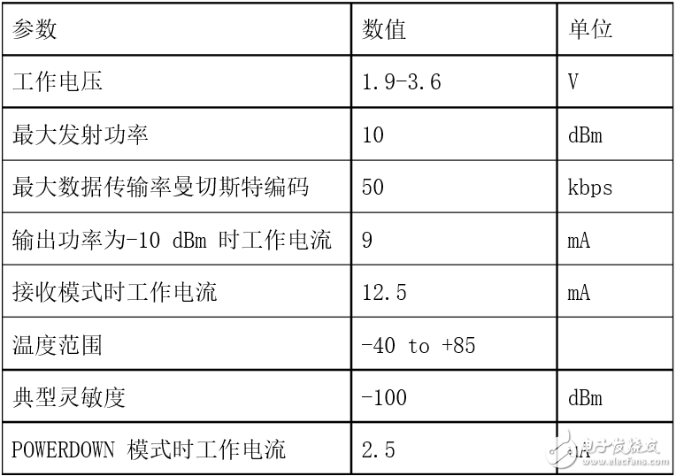
Working frequency band 422.4~473.5MHz
512 communication channels, meeting the needs of multi-point communication, grouping, frequency hopping, etc., channel switching time ≤ 6us
The transmit power can be set to: 10dBm, 6dBm, -2dBm and -10dBm
Connect to the MCU via the SPI interface
Support 50kbps transmission rate
ShockBurst transmission mode, automatically generate preamble and CRC check code
Operating voltage range: 1.9V ~ 3.6V, the current is only 12.5μA in standby mode
Operating temperature range: -40 ° C ~ +85 ° C
nRF905 pin diagram and pin description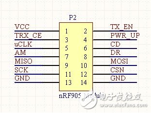
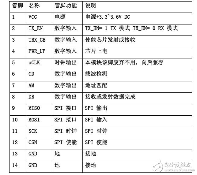
1. The voltage range of the VCC pin is between 1.9-3.6V. It cannot be outside this range. If it exceeds 3.6V, the module will be burned. Recommended voltage is about 3.3V;
2, the hardware does not have integrated SPI function of the microcontroller can also control this module, with ordinary single-chip IO port analog SPI timing for read and write operations;
3. The module interface adopts standard 2.54mmDIP pin, 13 pin and 14 pin are grounding pins, which need to be logically connected with the system circuit;
4. When connecting with the P0 port of the 51 series MCU, it is necessary to add a 10K pull-up resistor, and it is not required to connect with the remaining ports. For other series of 5V MCUs, such as AVR and PIC, please refer to the output current of the IO port of this series of MCU. If it exceeds 10mA, you need to connect 2-5K resistors in series, otherwise it is easy to burn the module! If it is a 3.3V MCU, it can be directly connected to the IO port.
1), mode control interface:
The interface consists of PWR, TRX_CE, TX_EN to control the four operating modes of the tuner consisting of nRF905: power down and SPI programming mode; standby and SPI programming mode; transmit mode; receive mode.
2), SPI interface:
The SPI interface consists of CSN, SCK, MOSI, and MISO. In the configuration mode, the MCU configures the operating parameters of the tuner through the SPI interface; in the transmit/receive mode, the MCU SPI interface transmits and receives data.
3), status output interface:
Provide carrier detect output CD, address match output AM, data ready output DR.
Pcb/Fpc Membrane Keypad,Membrane Keyboard,Fpc Membrane Keyboard,Customized Membrane Keypad
CIXI MEMBRANE SWITCH FACTORY , https://www.cnjunma.com