Abstract: Using the latest LDMOS FET devices, a balanced amplifier circuit structure is used to design a power amplifier in a digital TV transmitter. The working frequency range is from 470MHz to 860MHz, the gain in the whole frequency band is about 12dB, and it works in a linear state, and the intermodulation suppression is less than -35dB.
This article refers to the address: http://
Power amplifiers are an important part of digital TV transmitters. Normally, the signal in the digital television transmitter is modulated by the COFDM method and then output an intermediate frequency analog signal, which is sent to the amplifying portion by up-conversion. The modulation method includes two modes, IFFT (8M) and IFFT (2M), which are composed of 6817 and 1705 carriers, respectively. The frequency spacing between each carrier is very close, so the intermodulation signal can easily fall within the frequency band, causing crosstalk. Digital TV transmitters have higher requirements in terms of linearity and stability than traditional types. The power amplifier in the transmitter must be operated in a higher linear state and the gain is stable.
The amplified portion of the transmitting system is divided into an excitation and main amplification circuit. The excitation part is a broadband power amplifier. In order to ensure the normal stability of terrestrial digital TV transmission, it needs to have good stability and reliability. Its working frequency range is 470MHz~860MHz, the working state is AB class; the required gain is greater than 10dB, the intermodulation suppression Less than -35dB, the noise power density is greater than 130dBc/Hz. This article uses the latest LDMOS FET devices and balanced amplifier circuit structure. The driver-grade power amplifier in the digital TV transmitter is designed and optimized to meet system requirements.
1 power amplifier design
1.1 Amplifier chip selection of power amplifier
In this paper, Motorola LDMOS FET device MRF373 is used as the amplifier chip of the power amplifier. The chip has a large improvement in linearity, gain and output capability compared to BJT devices, which greatly improves the reliability and maintainability of the transmitter. Compared with traditional decimeter-wave bipolar power amplifier tubes, LDMOS FETs have the following significant advantages:
· Can work in high standing wave ratio (VSWR = 10:1);
· High gain (typically 13dB);
· Smooth saturation curve, which is beneficial to analog and digital TV RF signal amplification;
· Can withstand large overdrive power, especially suitable for COFDM modulated multi-carrier signals in DVB-T;
The bias circuit is simple and does not require complex active low impedance bias circuits with positive temperature compensation.
The LDMOS manufacturing process combines BPT and gallium arsenide processes. Unlike the standard MOS process, LDMOS does not use the BeO yttrium oxide isolation layer on the device package, but is directly bonded to the substrate. The thermal conductivity is improved, the device's high temperature resistance is improved, and the device lifetime is greatly extended. . Due to the negative temperature effect of the LDMOS tube, the leakage current automatically flows while being heated, and does not form a hot spot locally at the collector current as the positive temperature effect of the bipolar tube, so that the tube is not easily damaged. Therefore, the LDMOS tube greatly enhances the load mismatch and over-excitation tolerance. Also due to the automatic current sharing action of the LDMOS tube, its input-output characteristic curve is relatively gentle at 1dB compression point (saturation section of large signal application), so the dynamic range is widened, which is beneficial to analog and digital TV RF signal amplification. LDMOS is approximately linear in small signal amplification, with almost no intermodulation distortion, which greatly simplifies the correction circuit. The MOS device's DC gate current is almost zero, and the bias circuit is simple, eliminating the need for complex active low-impedance bias circuits with positive temperature compensation.
1.2 Circuit Structure Selection and Comparison
The small-signal S-parameter can be used in the design of a class A amplifier, which means that the amplification of the signal is basically limited to the linear region of the transistor. However, when it comes to high power amplifiers, small signals are usually nearly ineffective because the amplifier operates in a non-linear region. At this point, the large signal S-parameter or impedance of the transistor must be obtained to obtain a reasonable design effect.
Generally speaking, the Class A working state has the smallest distortion coefficient and good linearity. However, in the case of high power applications, it is not suitable due to the low efficiency (50%) of Class A operating conditions. Using the circuit form of a class A and B push-pull amplifier, a linear index similar to that of a class A amplifier can be obtained.
The push-pull circuit form consists of two independent single-tube amplifiers without any internal connections, with vector distribution and synthesis of power through two baluns. Because the balun itself has the characteristics of varistor, the impedance matching caused by the varistor ratio is greatly reduced, and the balun has a good suppression effect on even harmonics. However, since the spacing between the two sides of the balun is too small, the two paths have a large mutual influence, so the amplifier applying the balun structure has poor stability, and the input and output standing waves of the circuit are relatively poor.
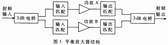
This article uses the form of a balanced amplifier, the structure shown in Figure 1. Its working principle is similar to that of the balun structure, but due to the application of the 3dB bridge, the isolation between the two RF signals is better, which is beneficial to the matching of the two ports. The advantages are shown in Table 1 with respect to the single-tube amplifier structure.
1.3 Matching network design
Since the MRF373 does not provide an internal match, a matching network is built in the amplifying circuit. The amplifying circuit in the digital television reflection system operates at 470 MHz to 860 MHz, and impedance matching is required in a wide frequency range. The basic idea of ​​the design of the wideband amplifier matching circuit is to use a reactive matching network for multi-stage impedance transformation between the input and output of the amplifier and the stage. The network only plays a matching role, no additional power loss, can guarantee the maximum transmission coefficient, balance the device characteristics, and can meet the bandwidth requirements of the system.
The load RL can be determined using the IV curve of the device or by parameters such as output power, operating voltage, and the like. To maximize output power, RL is used to represent the internal drain load of the device as a target for the output matching circuit. If a network has the best match for a complex impedance, the output impedance of the network is equal to the complex conjugate of the load impedance. The current load impedance is pure real RL, so the impedance of the optimal output matching circuit reflected to the device's drain load is the complex conjugate of RL, ie:
RL=(VDD-VDS(sat))2/2P
Where VDD is the operating voltage, VDS(sat) is the knee voltage, and P is the output power.
According to the above formula, the RL of the MRF373 is approximately 6 Ω.
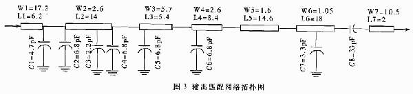
The amplifying circuit herein uses a method in which a separating element and a distributed parameter element are used in combination. Since inductors have higher heat losses than capacitors, inductors are often avoided in such circuits and replaced with high impedance transmission lines. A hybrid type of matching network typically includes several serially connected transmission lines and parallel capacitances in spaced configurations. The input matching part of the amplifier adopts four-section impedance transformation, and the output matching adopts a hybrid circuit of five-section impedance transformation. The input and output matching network topology diagram is shown in Figure 2 and Figure 3.

2 circuit optimization and simulation results
Since the digital television transmission system requires that the amplifying circuit must operate in a linear amplification state, it can be analyzed by a small signal S-parameter method. With the small signal S-parameter file provided by the device manufacturer, the small signal S-parameter simulation of the whole circuit can be performed by ADS to obtain small signal gain, port matching, isolation and stability factor K. Table 2 shows the S parameters of MRF373 at (Vce = 26V, Ic = 500 mA).
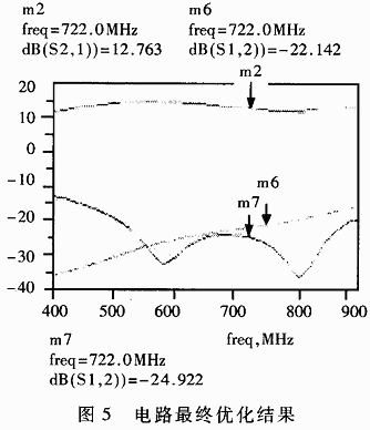
Circuit simulation with ADS does not meet the design requirements, and circuit optimization is required on this basis. When only the small-signal S-parameter is used as a model to design the power amplifier, the steps of circuit optimization are generally as follows: firstly, as far as possible, aiming at the matching of RL (load resistance of the maximum output power), optimizing and determining the value of the output matching circuit component; Optimize the component values ​​of the input matching circuit to improve the gain and input matching circuitry. It should be noted that before optimization, it is necessary to obtain the output circuit model as complete as possible, and then optimize it at the operating frequency to achieve the best match with RL. Figure 4 shows the simulation results of the amplifier circuit, and Figure 5 shows the final optimization results of the circuit.
3 test results
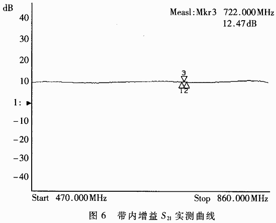
After a lot of experiments and repeated debugging, the measured results are shown in Figure 6. The driver stage amplifier operates in a linear state. As can be seen from the gain curve of Fig. 6, the gain in the entire frequency band is flat, about 12 dB, which is roughly the same as the simulation result. The return loss is less than 15 dB and the in-band standing wave ratio is less than 1.3. When the input power is 2 watts, the output power is 25W measured by the power meter, the signal amplitude is stable, and the cross-talk suppression is less than -35 dB. The indicators meet the system requirements, and are close to the indicators of amplifiers in similar digital TV transmitters abroad, and the cost is greatly reduced, which lays a foundation for the domestic development of digital TV transmitters in the future.
Antenna design for mobile reception terrestrial digital TV
1. Receiving digital TV on the move, because the signal changes with different geographical locations, and the channel characteristics are dynamically changed, which requires the antenna to reflect the stable reliability of the dynamic characteristics of different channels in real time, and the antenna in motion A certain bandwidth and gain must be guaranteed in a comprehensive range. To this end, we have designed a omnidirectional cylindrical spiral microstrip antenna that spirally winds a quarter-wavelength microstrip resonator on a hollow cylinder with a certain thickness (h). Coaxial cylinder with the floor, the volume is relatively short, can be conformed with any carrier (such as car), and can be designed to be connected to the coaxial cable in any size (50Ω, 75Ω), without matching the network, and the inside of the hollow core can be Install active electronics.
The medium having a certain thickness (h) is selected in order to increase the radiation conductance so that the Qr value and the total QT value corresponding to the radiation decrease, thereby increasing the bandwidth. When the dielectric substrate is selected, the dielectric constant εr and the loss tangent tan δ are simultaneously given. When εr is decreased, the "binding" of the medium is reduced. At this time, the antenna is easy to radiate, but relative to The energy storage of the antenna is reduced, the Qr value is decreased, and the frequency band is widened. However, the reduction of εr will increase the size of the dielectric substrate, and selecting a large loss tangent can widen the Qr drop band, but at this time, the antenna efficiency is A lot of reduction, so we must consider it. 
Since εr and tan δ are functions of frequency, the actual measurement is performed after selecting the dielectric substrate, so as to avoid the deviation of the position of the design feed point and affect the impedance matching. The dielectric material we chose was polytetrafluoroethylene (PTFE), which was formed by stamping at the design size, and then coated with wire and floor by evaporation and ion plating. 
2. Determination of the bandwidth of the microstrip 
Since the strip length λg/4 is related to εe (equivalent dielectric constant, λg=λ0/εe), when εr and h are known, W depends on εe and can be calculated according to the following formula: W=C*fr (εr+12)-12
Where fr——working frequency; 
C——the speed of light;
εr - relative dielectric constant. 
Digital TV generally works in the range of 470 to 860 MHz, with a bandwidth of 6 to 8 MHz and a gain of about 4 dB. When the width calculated by less than the above formula is selected, the antenna efficiency will be lowered, and although the efficiency is higher than that of the above formula, the high-order mode is likely to affect the sharpness of the image. In order to avoid complicated calculations in engineering, the W/h, εe, Z0 values ​​given in the microstrip antenna engineering manual can be found for the characteristic impedance of strips with different media and different sizes when designing microstrip lines. 
3. Correction of the spiral microstrip line
Because the terminal of the spiral microstrip line is open circuit, we theoretically think that the open circuit of the terminal has an infinite open load impedance. In fact, it is not a true open circuit. There is an edge effect of the electric field at the open end, which is equivalent to attaching a terminal to the terminal. The terminal capacitor, in order to offset the effect of this terminal capacitance, the open end is shortened by a Δl length than the ideal design calculation. Because the terminal load impedance is infinite, the input impedance of the λg/4 transmission line is zero. When the terminal load is connected with an additional capacitor, if the input impedance is still to be zero, the microstrip line is shortened by a Δl length. 
Because the λg/4 microstrip line is spirally wound around the cylinder, a mutation (sharpening) occurs at the end, and this mutation introduces an additional reactance, so the microstrip line is corrected for this mutation to offset this. The influence of a kind of reactance. 
The value of Δl removed by the correction value is related to the values ​​of W, h, and εr. It is extremely complicated to introduce many complex functions by using the microstrip line correction theory analysis and calculation. At the same time, many assumptions are given, and it is difficult to obtain accurate results. In actual work, it is necessary to repeat the experiment and accumulated experience to correct, Δl generally takes 0.2 times of the microstrip line. 
We designed the λg/4 spiral patch antenna to cut off the corner of the microstrip line to offset the terminal capacitance, add the influence of the reactance, and it can also fine-tune the resonant frequency. When the T1 is cut, the frequency will increase. The impact of the match is minimal. When the T2 is cut off, the frequency is also lowered, but the impedance has a great influence on the impedance and needs to be re-adjusted. Therefore, it is advantageous to design the resonant operating frequency slightly lower. In order to make the spiral microstrip antenna easy to radiate and receive, a certain distance of the radiation gap (B) is left at the edge. Experience has shown that when the spatial separation between the two bands (S) is at least half of the microstrip width (W), the antenna works best, so the number of spiral turns can be easily determined. To ensure the omnidirectional pattern, the microstrip width is not It should be smaller than the diameter of the cylinder (D). The feeding mode directly affects the radiation characteristics of the microstrip line. We use the 50Ω BNC type connector to feed back the output. The center line of the plug is connected with the feeding point of the microstrip line, and the grounding end is connected to the floor of the cylinder inner wall. In order to protect the spiral microstrip line from the external environment, a glass cover is placed on the outside of the spiral patch microstrip antenna to prevent rain and snow damage. A magnet is attached to the top of the antenna to attract the top of the car.
4, the conclusion 
China's development of digital TV started late, but the development speed is very fast, the market is particularly large, but the technical standards of its proprietary property rights are lacking. Although Tsinghua is developing the digital multimedia broadcasting terrestrial (DMB-T) standard, Jiaotong University is also developing advanced digital TV. The broadcast terrestrial (ADTB-T) standard, but still in the process of continuous improvement, China must have its own standards of independent intellectual property rights. At present, domestic manufacturers have the ability to provide DVB core equipment recognized by the industry, and also broadcast a number of digital TV channel pilot programs, so I hope relevant departments will announce China's own terrestrial digital video broadcasting standards as soon as possible to create better digital TV. The environment allows people to enjoy high-definition digital TV programs brought by high technology.
Earphone For Mobile Phone advantage:
Enriched sound and reliable quality in all aspects of their design,Strong bass generated from powerful driver,power and great sensitivity response,Their uniquely contoured body allow for a 45 degree in-ear angle which offers ergonomic comfort and noise isolation better than standard headphones,Stylish color design with mic and volume controller, CE and FCC marks, EN71, WEEE, ROHS AND REACH IF NEEDED
Earphone For Mobile Phone
Earphone For Mobile Phone,Plug Double Online Headphones,Bluetooth Headset,Stereo Headphone
Dongguan City Leya Electronic Technology Co. Ltd , https://www.dgleya.com