The constant voltage/constant current output single-chip switching power supply can be simply referred to as a constant voltage/constant current source. It features two control loops, one for the voltage control loop and the other for the current control loop. When the output current is small, the voltage control loop acts and has a voltage regulation characteristic, which is equivalent to a constant voltage source; when the output current approaches or reaches the rated value, the IO is kept constant through the current control loop, and it becomes a constant current source again. . This power supply is especially suitable for battery chargers and special motor drives. The following describes a low-cost constant voltage/constant current output switching power supply whose current control loop is composed of transistors, which is simple in circuit, low in cost, and easy to manufacture.
1. The working principle of constant voltage / constant current output switching power supply
The circuit of the 7.5V, 1A constant voltage / constant current output switching power supply is shown in Figure 1. It uses a TOP200Y type switching power supply (IC1) with a PC817A linear optical coupler (IC2). The 85V~256V AC input voltage u passes through the EMI filters L2, C6), the rectifier bridge (BR) and the input filter capacitor (C1) to obtain a DC high voltage UI of approximately 82V to 375V, and then the drain of the TOP200Y is connected through the primary winding. The drain clamp protection circuit composed of VDZ1 and VD1 limits the peak voltage formed by the leakage inductance of the high-frequency transformer to a safe range. VDZ1 uses BZY97-C200 transient voltage suppressor with clamping voltage UB=200V. VD1 selects UF4005 ultra-fast recovery diode. After the secondary voltage is rectified and filtered by VD2 and C2, it is filtered by L1 and C3 to obtain +7.5V output. The VD2 uses a 3A/70V Schottky diode. After the output voltage of the feedback winding is rectified and filtered by VD3 and C4, the feedback voltage UFB=26V is obtained, and the phototransistor is biased. C5 is a bypass capacitor that doubles as a frequency compensation capacitor and determines the automatic restart frequency. R2 is the dummy load of the feedback winding, which can limit the feedback voltage UFB from rising when no load is applied. 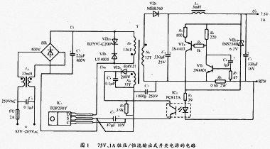
The power supply has two control loops. The voltage control loop is composed of a 1N5234B type 6î€2V regulator (VDZ2) and an optocoupler PC817A (IC2). Its function is to make the switching power supply operate in the constant voltage output mode when the output current is small. At this time, there is current flowing through the VDZ2. The output voltage is regulated by the voltage regulation value of the VDZ2 (UZ2) and the forward voltage drop (UF) of the LED in the optocoupler. determine. The current control loop is composed of transistors VT1 and VT2, current detecting resistor R3, optocoupler IC2, resistors R4 to R7, and capacitor C8. Among them, R3 is dedicated to detecting the output current value. VT1 adopts 2N4401 type NPN silicon tube, domestic substitute model is 3DK4C; VT2 selects 2N4403 type PNP silicon tube, which can be replaced by domestic 3DK9C. R6 and R5 are used to set the collector current values ​​IC1 and IC2 of VT1 and VT2, respectively. R5 also determines the DC gain of the current control loop. C8 is a frequency compensation capacitor to prevent self-oscillation of the loop. When power-on or automatic restart, the transient peak voltage can make VT1 turn on, and use R7 to limit its emitter junction current; R4 is used to bypass the VT1 turn-on current through VT2, so that it does not pass R1. . The starting process of the current control loop is as follows: As IO increases, when IO is close to 1A, UR3↑→VT1 is turned on→UR6↑→VT2 is turned on, and the collector of VT2 supplies current to the optocoupler, forcing UO↓ . Reduced by UO, VDZ2 can not be reversed in reverse, and no current flows through it. Therefore, the voltage control loop is open and the switching power supply automatically switches to constant current mode. C7 is a safety capacitor that filters out common-mode interference caused by the primary and secondary coupling capacitors.
The power supply operates from a 7.5V regulated output and operates at a controlled current of 1A. When the ambient temperature range is 0 ° C ~ 50 ° C, the accuracy of the constant current output is about ± 8%.
The output voltage-output current (U0-I0) characteristics of this power supply are shown in Figure 2. As can be seen from the figure, it has the following salient features:
(1) When u=85VAC or 265VAC, the characteristic curve changes little, which indicates that the output characteristics are not affected by the change of the AC input voltage;
(2) When the IO<0.90A is in the constant voltage region, the IO≈0.98A is in the constant current region, and the UO decreases rapidly with the slight increase of IO;
(3) When UO≤2V, VT1 and VT2 can no longer supply enough working current to the optocoupler. At this time, the current control loop does not work, but the primary current is still limited by the maximum limit current ILIMIT(max) of TOP200Y. At this time, UR6↑, the optocoupler operating current is rapidly reduced by VT1 and VT2, forcing the TOP200Y to enter the automatic restart state. This shows that once the current control loop is out of control, it immediately switches from the constant current mode to the automatic restart state, pulling the IO down to protect the chip.
2. Circuit design of constant voltage / constant current output switching power supply
The unit circuit of the voltage and current control loop is shown in Figure 3.
2.1 Design of voltage control loop
The output voltage of the constant voltage source is determined by:
UO=UZ2+UF+UR1=UZ2+UF+IR1·R1(1)
Where UZ2 = 6.2V, UF = 1.2 (typical), all that needs to be determined is the voltage drop UR1 on R1. Let the current on R1 be IR1, the collector current of VT2 be IC2, the optocoupler input current (ie LED operating current) be IF, obviously IR1=IC2=IF, and their current transfer ratio CTR value with u, IO and optocoupler And change. The control current IC of TOP200Y varies from 2.5mA (corresponding to the maximum duty cycle Dmax) to 6.5mA (corresponding to the minimum duty cycle Dmin), and the intermediate value IC = 4.5mA. Since the IC flows from the emitter of the phototransistor to the control terminal, it has a relationship.
IR1=Ic/CTR (2)
After the IC and CTR values ​​are determined, it is easy to find IR1. The monolithic switching power supply must use a linear optocoupler, which requires CTR=80%~160%, and the intermediate value is 120%. IC=4.5 mA, CTR=120% is substituted into equation (2), and IR1=3.75 mA. When R1=39Ω, UR1=0.146V. The last substitution is calculated in (1)
UO=UZ2+UF+UR1=6.2V+1.2V+0.146V
=7.546V≈7.5V
2.2 Design of current control loop
The current control loop is composed of VT1, VT2, R1, R3 to R7, C8, and PC817A. Next, the expected value of the constant output current IOH needs to be finally calculated. In Figure 3, R7 is the base bias resistor of VT1. Since the base current is small and the current on R3 is large, it can be considered that the emitter junction voltage drop UBEI of VT1 falls on R3. then
IOH=UBE1/R3 (3)
The emitter junction voltage drop of VT1 and VT2 can be estimated by the following two formulas:
UBE1=(kT/q)·In(Ic1/Is) (4)
UBE2=(kTq)·In(Ic2/Is) (5)
Where k is the Boltzmann constant, T is the ambient temperature (expressed by thermodynamic temperature), and q is the electron charge. When TA = 25 ° C, T = 298 K, kT / q = 0.0262V. IC1 and IC1 are the collector currents of VT1 and VT2, respectively. IS is the reverse saturation current of the transistor. For small power tubes, IS = 4 x 10-14A.
Since IR1=IF=IC2=3.75mA has been found before, UBE2=(kT/q)In(Ic2/Is)
=0.0262In(3.75mA/4×10 -14A)
=0.662V
Since IE2 ≈ IC2, UR5=IC2R5=3.75 mA×100 Ω=0.375 V, from which UR6=UR5+UBE2=0.375V+0î€662=1.037V is derived. When R6=220Ω, IR6=IC1=UR6/R6=4.71mA. This value is used to estimate UBE1 to determine the resistance of current sense resistor R3:
UBE1=0.0262In(4.71mA/4×10 -14A)=0.668
R3=IBE1/IOH=0.668V/1.0A=0.668Ω
The closest nominal resistance is 0.68 Ω. Substitute (3) can be obtained
IOH=0.668V/0.68Ω=0.982
Considering the temperature coefficient αT≈-21mV/°C of the emitter junction voltage UBE1 of VT1, when the ambient temperature rises by 25°C, the IOH value drops to
I'OH=UBE1-‖αT‖·T/R3
=0.668V-(2.1mV/°C)×25°C/0.68Ω=0.905A
Constant current accuracy is
γ=(I'OH-IOH/IOH)·100%
=(0.905-0.982/0.982)·100%=-7.8%≈-8%
Consistent with the design indicators.
3. Feedback power supply design
The design of the feedback power supply mainly includes two contents:
(1) Calculate the number of turns NB of the feedback winding in constant current mode. The reason why the NB value is calculated in the constant current mode is because both UO and UFB are rapidly reduced (UO=UOmin=2V), and only when the UFB is high enough can the constant current source be operated normally.
(2) Calculate the feedback voltage rating UFB in the constant voltage mode. At this time, UO=7.5V, UFB will also reach the maximum value, thereby obtaining the UFB value, which can provide a basis for selecting the withstand voltage value of the optocoupler.
The feedback voltage UFB is determined by:
UFB=(Uo+UF2+IoR3)·NB/Ns-UF3 (6)
In the formula, UF2 and UF3 are the forward voltage drop of VD2 and VD3, respectively. NS is the secondary number. Can be solved from equation (6)
NB=(UFB+UF3/Uo+UF2+IoR3)·Ns (7)
In the constant current mode, when the load is increased (ie, the load resistance is reduced), UO and UFB are automatically reduced to maintain the constant current output. In order to make the switching power supply from the constant current mode to the automatic restart state, it can still provide the proper bias voltage to the TOP200Y, and the UFB is required to be at least 3V higher than the maximum value UCmax of the control voltage in the constant current mode. It is assumed here that UCmax = 6V, so UFB = 9V is taken. UFB=9V, UO=UCmin=2V, UF2=0î€6V, UF3=1V, IO=IOH=0.982A, R3=0.68Ω, NS=12åŒ are substituted into equation (7), and NB=36.7 is calculated.åŒâ‰ˆ37åŒ (rounded up).
In the constant voltage mode, UO=7.5V, the maximum output current IO=0.95A, and then substituted into equation (6), UFB=26V, which is the rated value of the feedback voltage. When optocoupler is selected, the reverse breakdown voltage of the phototransistor must be greater than this value, ie U(BR)CEO>26V. Commonly used linear optocoupler U(BR) CEO=30V~90V. The formula for calculating the reverse working voltage UIC2 of the phototransistor is
UIC2=UFB-UCmin (8)
Where UCmin is the minimum value of the control terminal voltage (5.5V). It is not difficult to calculate, UIC2 = 20.5V. Here, the PC817A type optical coupler is used, and its U(BR)CEO=35V>20.5V can fully meet the requirements. However, when designing a high-voltage battery charger, a high-voltage optocoupler must be selected.
(Edit: Bright)
Phenolic Cotton Cloth Laminate
Phenolic Cotton Cloth Tube,Paper Based Bakelite Tube,Phenolic Cotton Cloth Laminated Tube
Zhejiang Jingjing Insulation Materials Co., Ltd. , http://www.zjepoxyglasssheet.com